A preparation method of deep hole interconnection structure based on nanometer metal

A technology of nano-metal and interconnection structure, applied in the direction of nano-technology, semiconductor/solid-state device manufacturing, electrical components, etc., can solve the problems of environmental pollution and environmental pollution, and achieve the effect of avoiding pollution

Active Publication Date: 2022-04-19
GUANGDONG UNIV OF TECH
View PDF7 Cites 0 Cited by
  • Summary
  • Abstract
  • Description
  • Claims
  • Application Information

AI Technical Summary

Problems solved by technology

[0004] The packaging technology of TSV vertical interconnection is mainly to open TSV holes on the back of the wafer to expose the pads, use the metal layer to lead the pads to leads, and then wire and ball plant on the back of the wafer. Most of the existing TSV processes use electroplating. The copper process forms a conductor structure, but the copper electroplating process will cause great pollution to the environment, which is not environmentally friendly
For example, the Chinese patent with the announcement number CN105405781A and the publication date of March 16, 2016: the method of manufacturing the back leads of the wafer-level package by using the CMP process. Great pollution to the environment

Method used


Image

  • A preparation method of deep hole interconnection structure based on nanometer metal
  • A preparation method of deep hole interconnection structure based on nanometer metal
  • A preparation method of deep hole interconnection structure based on nanometer metal

Examples


Embodiment 1

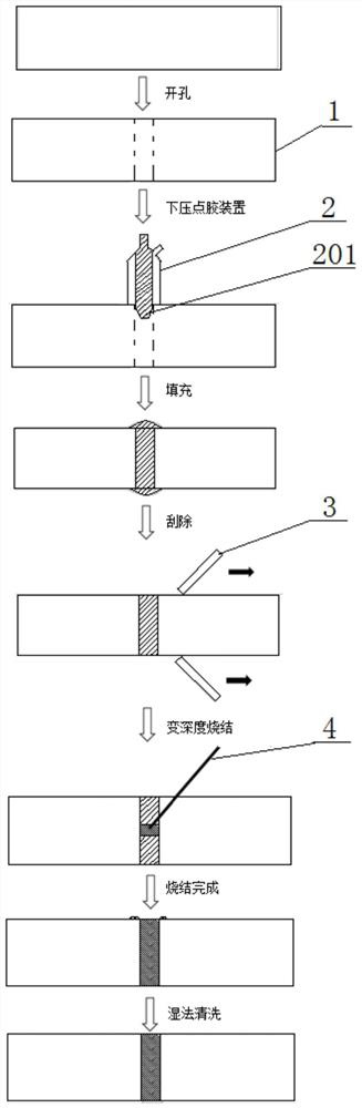
[0047] Such as figure 1 As shown, a method for preparing a deep-hole interconnection structure based on nanometer metal, for an interconnection structure in which the deep hole is a through hole, comprises the following steps:

[0048] S1. Using laser processing or physical cutting or chemical etching to form through holes on the glass plate 1 to be formed with a deep hole interconnection structure;

[0049] S2. Move the dispensing device 2 to the through hole facing the glass plate 1, press down the dispensing device 2, and the dispensing head 201 of the dispensing device 2 extends into the through hole to seal the through hole, and then the nano-metal The paste is squeezed into the through hole, and then the automatic optical inspection system is used to judge whether the nano metal paste is completely filled in the through hole. When the through hole is not completely filled, continue to squeeze the nano metal paste into the through hole. When the through hole is completely...

Embodiment 2

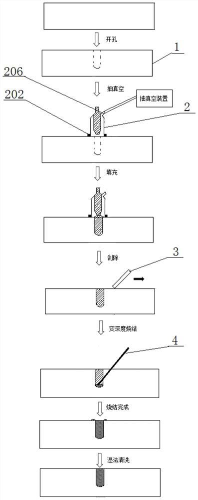
[0074] refer to figure 1 For example, a method for preparing a deep hole interconnection structure is provided. For an interconnection structure in which the deep hole is a through hole, the following steps are included:

[0075] S1, using CO with a wavelength of 10.6 μm, a pulse width of 500 ps, ​​a frequency of 5 Hz, and a power of 5 mJ 2 Laser, processing a through hole with a diameter of 1.2 μm on the glass plate 1, the through hole is perpendicular to the surface of the glass plate 1, penetrates the upper and lower surfaces, the cross section of the through hole is circular, and the depth is 70 μm;

[0076] S2. Move the dispensing device 2 to the through hole facing the glass plate 1, press down the dispensing device 2, and the dispensing head 201 of the dispensing device 2 extends into the through hole until one end of the through hole is sealed and squeezed The nano-copper paste in the dispensing head 201 makes the nano-copper paste fill in the through hole. The shape ...


PUM

PropertyMeasurementUnit
particle diameteraaaaaaaaaa

Abstract

The invention discloses a method for preparing a deep-hole interconnection structure based on nanometer metal. Firstly, a deep hole is formed on a glass plate to be formed with a deep-hole interconnection structure; After the completion, scrape off the residual nano-metal particles overflowing from the surface of the glass plate; then carry out variable-depth sintering on the filled nano-metal; The joint structure is prepared. In the present invention, the deep holes are filled with nanometer metals, and then sintered to form a conductor structure interconnected in the deep holes, without the need for electroplating copper, thereby avoiding environmental pollution.

Description

technical field [0001] The invention relates to the technical field of semiconductors, in particular to a method for preparing a nano-metal-based deep hole interconnection structure. Background technique [0002] The size of integrated circuits can be reduced to the nanometer level, which is gradually approaching the physical limit of size. The method of reducing the feature size can no longer improve the performance and function of integrated circuits. Therefore, the development of integrated circuits is facing a series of problems and challenges. [0003] At present, three-dimensional integration technology is used to solve the above problems. Compared with traditional planar circuits, three-dimensional integration technology stacks and integrates chips in the vertical direction, and improves the integration of circuits without further reducing the feature size of devices. Spend. Three-dimensional integration technology can integrate chips of various materials, processes ...

Claims


Application Information

Patent Timeline
Patent Type & Authority Patents(China)
IPC IPC(8): H01L21/768B82Y40/00
CPCH01L21/76877H01L21/76864B82Y40/00
Inventor 孙斐杨冠南刘宇崔成强张昱
Owner GUANGDONG UNIV OF TECH
Why Eureka
Try Eureka