Power MOSFET with Miller clamping function

A Miller clamp and functional technology, applied in the direction of electrical components, electric solid devices, circuits, etc., can solve the problems of device burning, upper and lower tubes through short circuit, device mis-opening, etc.

Active Publication Date: 2021-05-14
NOVUS SEMICON CO LTD
View PDF11 Cites 5 Cited by
  • Summary
  • Abstract
  • Description
  • Claims
  • Application Information

AI Technical Summary

Problems solved by technology

[0003] However, the higher switching speed brings about the increase of dv / dt, especially in the bridge circuit, the rapid change of the Switch node voltage will cause the Miller capacitance in the power MOSFET to charge and discharge rapidly, and the charge and discharge current will pass through The peripheral driving circuit forms a potential difference between the gate and the source of the power MOSFET. This potential difference reaches a certain level, which will cause the device to be turned on by mistake, so that the upper and lower tubes will be short-circuited, and the device will eventually burn out.

Method used


Image

  • Power MOSFET with Miller clamping function
  • Power MOSFET with Miller clamping function
  • Power MOSFET with Miller clamping function

Examples


Embodiment Construction

[0034] The principles and features of the present invention are described below in conjunction with the accompanying drawings, and the examples given are only used to explain the present invention, and are not intended to limit the scope of the present invention.

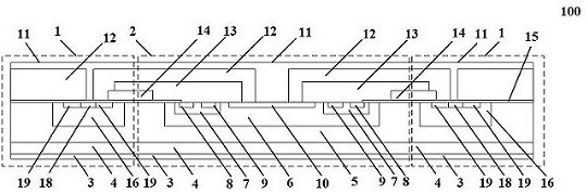
[0035] Such as Figure 2-Figure 3 As shown, a power MOSFET with Miller clamping function provided by the first embodiment of the present invention includes a BJT for Miller clamping, and MOSFET cells 1 arranged on both sides of the BJT;

[0036] The BJT includes a drain metal 3, an N+ type substrate 4 and an N-type epitaxial layer 5 stacked sequentially from bottom to top;

[0037] The top layer of the N-type epitaxial layer 5 has a first P-type well region 6, and the top layer of the first P-type well region 6 has an N-type well region 7 and a first P+ ohmic contact region 10 arranged at intervals, The N-type well region 7 is located on both sides of the first P+ ohmic contact region 10; the N-type well region 7 h...


PUM


Abstract

The invention relates to a power MOSFET with a Miller clamping function, and belongs to the technical field of power semiconductor devices. According to the power MOSFET (insulated gate field effect transistor) with the Miller clamping function, charging and discharging current on a Miller capacitor can be discharged to a source electrode through a monolithic integrated BJT (bipolar transistor), and only a small amount of gate-source voltage drop is generated, so that the risk that the power MOSFET is started by mistake due to charging and discharging of the Miller capacitor is effectively reduced, and the short-circuit robustness of the device is greatly improved.

Description

technical field [0001] The invention belongs to the technical field of power semiconductor devices, and in particular relates to a power MOSFET with a Miller clamp function. Background technique [0002] Power MOSFETs are widely used in the field of power electronics. Compared with bipolar devices (such as IGBTs), power MOSFETs have lower switching losses, which makes them more competitive in high-frequency application scenarios. [0003] However, the higher switching speed brings about the increase of dv / dt, especially in the bridge circuit, the rapid change of the Switch node voltage will cause the Miller capacitor in the power MOSFET to charge and discharge rapidly, and the charge and discharge current will pass through The peripheral drive circuit forms a potential difference between the gate and source of the power MOSFET. This potential difference reaches a certain level, which will cause the device to be turned on by mistake, so that the upper and lower tubes are sho...

Claims


Application Information

Patent Timeline
Patent Type & Authority Applications(China)
IPC IPC(8): H01L27/07
CPCH01L27/0705
Inventor 顾航高巍戴茂州
Owner NOVUS SEMICON CO LTD
Why Eureka
Try Eureka