
Silicon wafer cutting device and method

A cutting device, a technology for silicon wafers, applied in laser welding equipment, electrical components, circuits, etc., can solve the problem of low smoothness of silicon wafer cutting end face, slag accumulation, and control of silicon wafer cutting line width and depth Failure to meet requirements, etc.

Pending Publication Date: 2021-05-18
HANS LASER TECH IND GRP CO LTD
View PDF13 Cites 3 Cited by
  • Summary
  • Abstract
  • Description
  • Claims
  • Application Information

AI Technical Summary

Problems solved by technology

[0005] The object of the present invention is to provide a silicon wafer cutting device and method to solve the problem in the prior art that when laser scribing is used to cut silicon wafers, slag accumulation is easy to occur, resulting in a wide cutting line width of silicon wafers. and the control of the depth cannot meet the requirements, and the smoothness of the silicon wafer cutting end face is not high

Method used


Image

  • Silicon wafer cutting device and method
  • Silicon wafer cutting device and method
  • Silicon wafer cutting device and method

Examples


Embodiment Construction

[0042] In order to make the technical problems, technical solutions and beneficial effects to be solved by the present invention clearer, the present invention will be further described in detail below in conjunction with the accompanying drawings and embodiments. It should be understood that the specific embodiments described here are only used to explain the present invention, not to limit the present invention.

[0043] It should be noted that when an element is referred to as being “fixed” or “disposed on” another element, it may be directly on the other element or be indirectly on the other element. When an element is referred to as being "connected to" another element, it can be directly connected to the other element or indirectly connected to the other element.

[0044] It is to be understood that the terms "length", "width", "top", "bottom", "front", "rear", "left", "right", "vertical", "horizontal", "top" , "bottom", "inner", "outer" and other indicated orientations...


PUM


Abstract

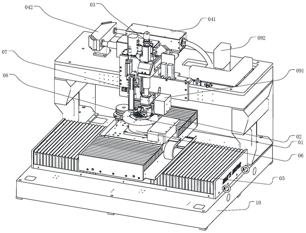
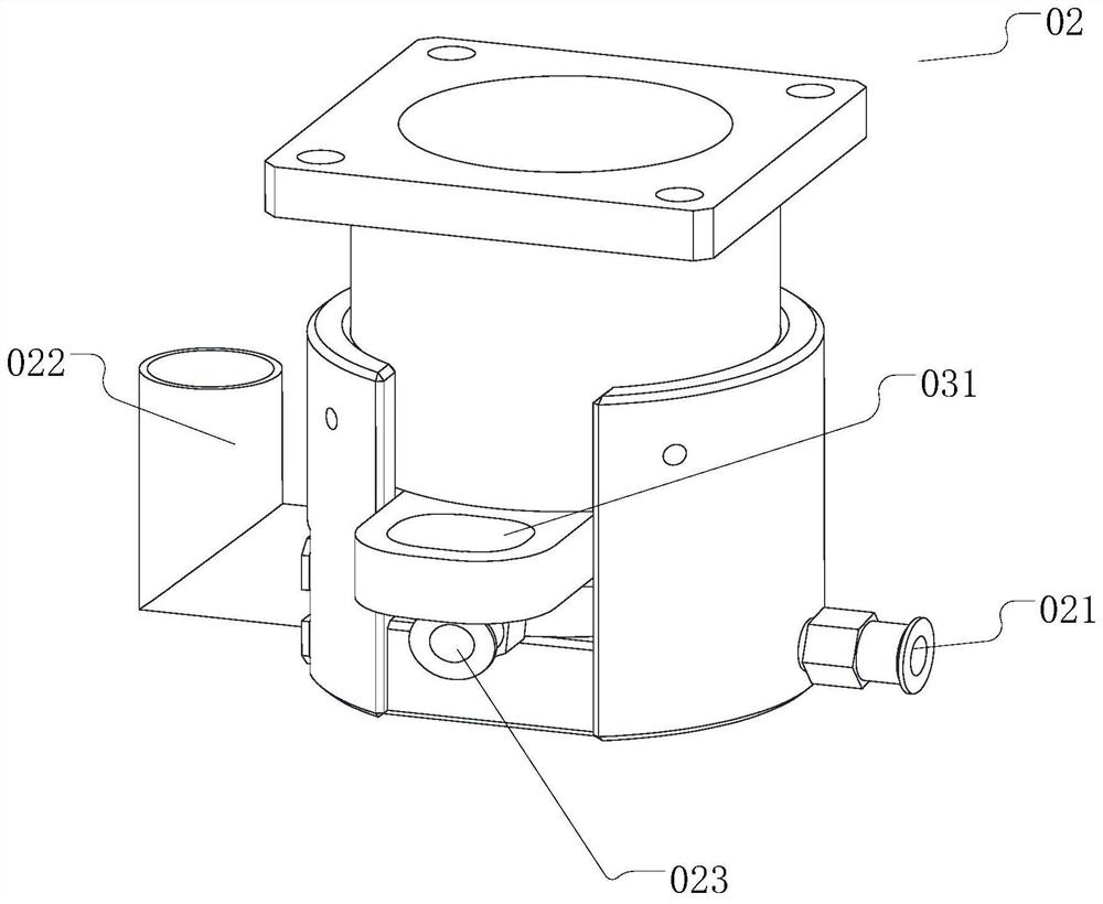
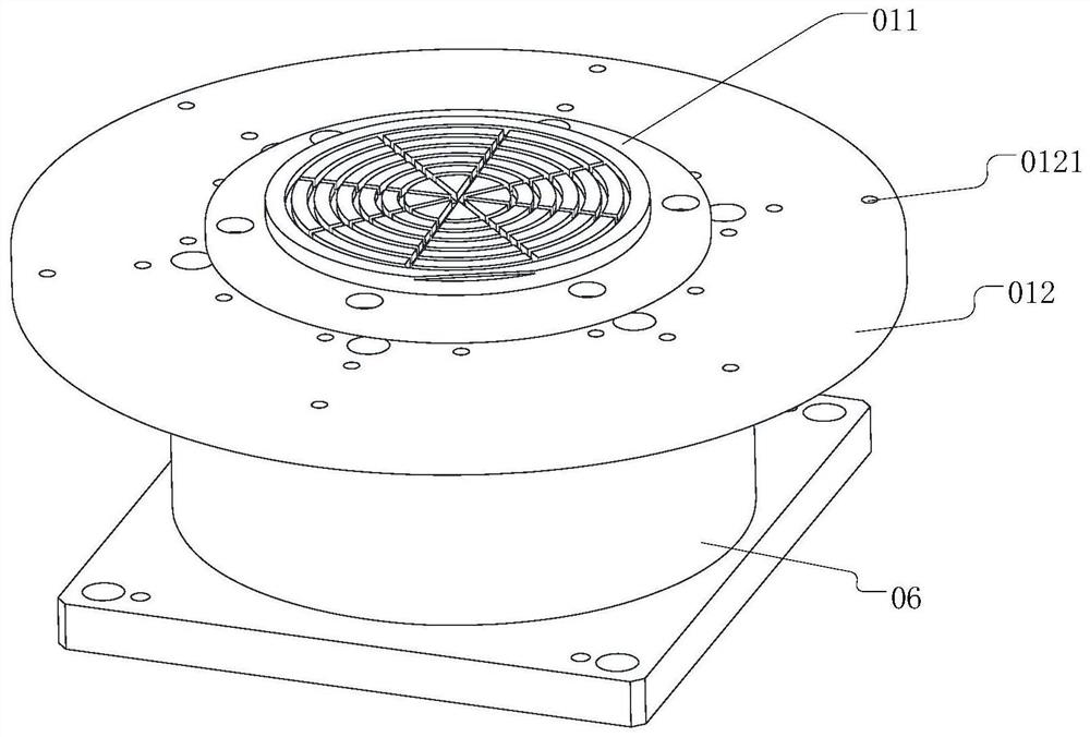
The invention relates to the field of laser cutting, and discloses a silicon wafer cutting device and method. The silicon wafer cutting device comprises a laser beam module, a wafer fixing module, an air blowing and dust exhausting module and a kerf observation module; the laser beam module is provided with a laser emitting end, the air blowing and dust exhausting module comprises a side air blowing port, a direct air blowing port and a dust exhausting port, and the side air blowing port and the dust exhausting port are formed at the two opposite sides of the laser emitting end; the direct air blowing port is used for generating airflow towards a silicon wafer, the side air blowing port is used for generating airflow flowing to the dust exhausting port, and the dust exhausting port is used for generating negative pressure within a specified pressure range so that dust can be discharged from the dust exhausting port; and the kerf observation module is used for observing or acquiring an image of a cutting part of the silicon wafer. According to the silicon wafer cutting device, dust generated during laser cutting is effectively removed by arranging the air blowing and dust exhausting module, dust adhering near a kerf is prevented, and meanwhile precise machining of a silicon wafer is achieved by arranging the kerf observation module.

Description

technical field [0001] The present invention relates to the field of laser cutting, and more specifically relates to a silicon wafer cutting device and method. Background technique [0002] Silicon wafers are brittle materials with high hardness and high brittleness. The traditional method of cutting silicon wafers is mainly to use the high-speed rotating knife wheel for scribing. However, the knife wheel cutting method has many disadvantages, such as low efficiency, large chipping at the cutting edge, and uneven edges, etc., which often affect the quality of the product. Rate. The cutter wheel used is easy to wear and needs to be replaced regularly. [0003] Laser scribing and cutting is a kind of laser irradiating on the workpiece with high energy density. The concentrated laser energy acts on the workpiece to be processed, so that the processed part heats up rapidly, and the processed part melts and vaporizes, forming cavities and cavities. Slits are formed as the lase...

Claims


Application Information

Patent Timeline
IPC IPC(8): B23K26/16B23K26/38B23K26/402B23K26/70H01L21/304
CPCB23K26/16B23K26/38B23K26/402H01L21/3043B23K26/702
Inventor 林家新焦波郑盼温尧明覃忠贤谢圣君吕启涛高云峰
Owner HANS LASER TECH IND GRP CO LTD
Learn More