
Semiconductor power device test heating table

A technology of power devices and semiconductors, which is applied in the field of semiconductor power device test heating tables, and can solve problems such as different heating speeds, inconsistent environmental conditions of semiconductor power devices, and uneven heating

Pending Publication Date: 2021-05-18
浙江大学绍兴微电子研究中心 +2
View PDF0 Cites 0 Cited by
  • Summary
  • Abstract
  • Description
  • Claims
  • Application Information

AI Technical Summary

Problems solved by technology

However, in actual use, there will be problems such as different heating speeds at each position, uneven heating, and large differences in temperature distribution.
The existence of the above problems will lead to inconsistent environmental conditions during the test of semiconductor power devices, causing the test results to exceed the error range

Method used


Image

  • Semiconductor power device test heating table
  • Semiconductor power device test heating table
  • Semiconductor power device test heating table

Examples


Embodiment 1

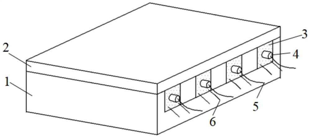
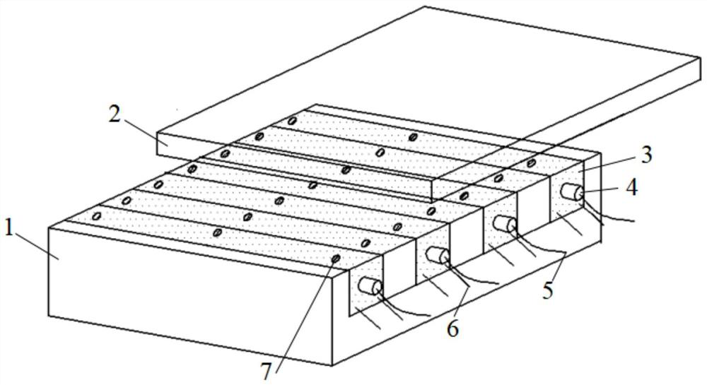
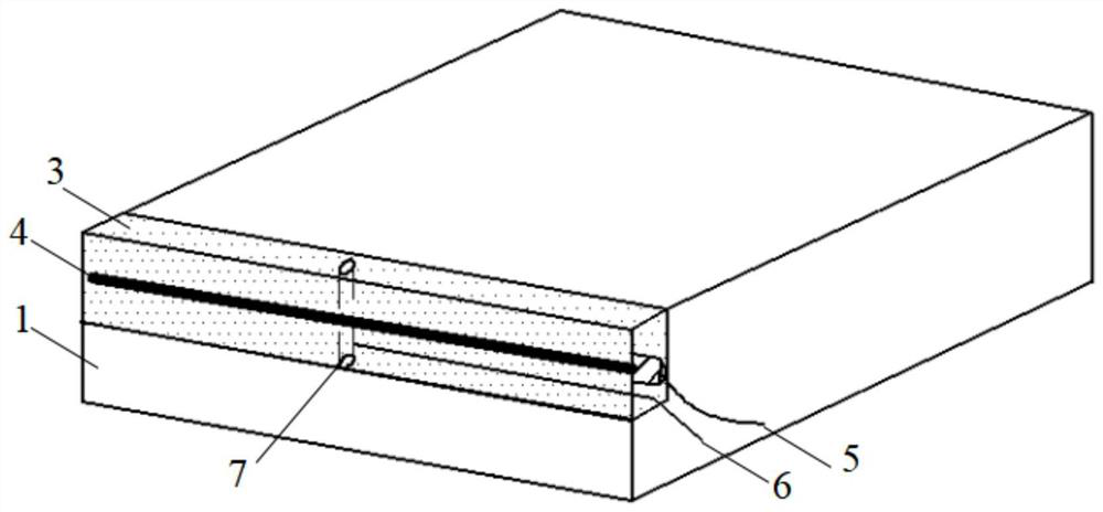
[0026] A test heating table for semiconductor power devices, used for heating during test and analysis of semiconductor devices, combined with the attached Figure 1-6 As shown, the structure of the heating platform includes: light metal layer 1; ceramic layer 2; filled with thermally conductive material 3; out). In this embodiment, the heating element 4 is an iron-chromium-aluminum heating wire, the temperature probe 7 is a Pt10 temperature probe, and the heat-conducting material 3 is filled with a heat-conducting resin.

[0027] The power controller provides the external voltage and current required by the heating table, and the voltage, current and temperature of each position of the heating table can be viewed on the controller display.

[0028] Among them, the heating platform adopts an upper and lower two-layer structure, and the upper ceramic layer 2 is a thin layer of ceramic Al 2 o 3 , with a thickness of 2mm, the lower light metal layer 1 is made of light metal al...

Embodiment 2

[0032] A test heating table for semiconductor power devices, used for heating during test and analysis of semiconductor devices, combined with the attached Figure 1-6 As shown, the structure of the heating platform includes: light metal layer 1; ceramic layer 2; filled with thermally conductive material 3; out). In this embodiment, the heating element 4 adopts nickel-chromium heating wire, the temperature probe 7 adopts a Pt100 temperature probe, and the filling heat-conducting material 3 adopts heat-conducting glue.

[0033] The power controller provides the external voltage and current required by the heating table, and the voltage, current and temperature of each position of the heating table can be viewed on the controller display.

[0034] Among them, the heating table adopts a two-layer structure, the upper ceramic layer 2 is a thin layer of ceramic AlN with a thickness of 4mm, and the lower light metal layer 1 is made of light metal stainless steel to reduce the weigh...


PUM

PropertyMeasurementUnit
thicknessaaaaaaaaaa
thicknessaaaaaaaaaa
thicknessaaaaaaaaaa

Abstract

The invention discloses a semiconductor power device test heating table which sequentially comprises a ceramic layer and a light metal layer from top to bottom, and the thickness of the ceramic layer is not larger than 5 mm. A plurality of strip-shaped grooves are evenly formed in the upper surface of the light metal layer, a heating element and a plurality of temperature probes are arranged in each strip-shaped groove, the heating elements are embedded in the length direction of the strip-shaped grooves, the temperature probes are evenly embedded in the length direction of the strip-shaped grooves, and the temperature probes are in contact with the bottom surface of the ceramic layer. The gaps in the strip-shaped grooves are filled with a filling heat conduction material. A clamp used for clamping a semiconductor device is arranged above the ceramic layer, and a heat conduction material is applied between the semiconductor device and the ceramic layer during use. The heating table is light in weight and convenient to move. The temperature distribution is uniform, accurate and controllable, the temperature adjustment is rapid, and the accurate test of the semiconductor device is facilitated.

Description

technical field [0001] The invention relates to a semiconductor power device testing heating platform, which belongs to the technical field of semiconductor device heating equipment. Background technique [0002] When testing and analyzing semiconductor devices in the laboratory, it is necessary to use a heating platform for heating to create the required working environment and maintain a constant temperature accurately. In order to ensure that the heat capacity of the heating table is large enough, the existing heating table on the market usually uses a thick metal block as the main body. However, in actual use, there will be problems such as different heating speeds at different positions, uneven heating, and large differences in temperature distribution. The existence of the above problems will lead to inconsistent environmental conditions during the testing process of semiconductor power devices, causing the test results to exceed the error range. Contents of the inv...

Claims


Application Information

Patent Timeline
Patent Type & Authority Applications(China)
IPC IPC(8): G01R31/26G01R1/04H05B3/02H05B3/06
CPCG01R31/2601G01R1/04H05B3/02H05B3/06
Inventor 胡建力林氦邓志江
Owner 浙江大学绍兴微电子研究中心
Learn More