
Communication method and communication system of interconnected die and DSP/FPGA
A communication system and bare core technology, applied in the field of communication systems, can solve problems such as poor flexibility and poor reconfigurability
- Summary
- Abstract
- Description
- Claims
- Application Information
AI Technical Summary
Problems solved by technology
Method used
Image

Examples
Embodiment 1
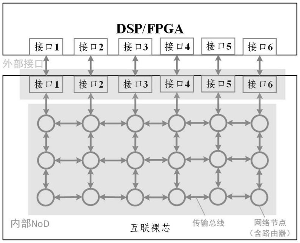
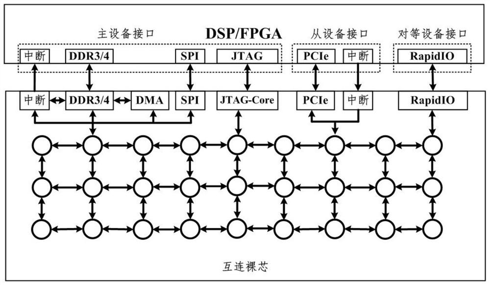
[0019] Such as figure 1 and figure 2 As shown, the communication method between the interconnected bare core and DSP / FPGA includes a plurality of data interfaces, each of which is provided with a different protocol conversion module, and the data interface includes data input conversion and data output conversion during communication; When the data input is converted, the external data of the DSP / FPGA is converted into a unified data protocol format by the protocol conversion module and transmitted to the bare core level network inside the interconnected bare core for unified data transmission; when the data output is converted, the interconnected bare core The internal data inside the core is converted into different data protocol formats by the protocol conversion module according to the data nature of the data itself, and enters different data interfaces for transmission to DSP / FPGA.
[0020] Such as figure 1 As shown, the interior of the interconnected bare core is an i...
Embodiment 2
[0023] Such as figure 1 and figure 2 As shown in the communication system of the interconnected bare core and DSP / FPGA, the interconnected bare core is provided with a plurality of data interfaces, and a plurality of the data interfaces are used to connect with the DSP / FPGA, and each of the data interfaces is provided with a different A protocol conversion circuit, the protocol conversion circuit is used to convert different external data into a unified data protocol format into the interconnected bare core and convert the internal data of the interconnected bare core into a corresponding data interface according to the purpose of the data data protocol format.
[0024] The data interface includes a master interface, a slave interface, and a peer interface.
[0025] The master device interface includes: an interrupt interface, a DDR data interface, an SPI interface and a JTAG interface, and the interrupt interface is used to receive an interrupt request from the interconnec...
PUM
 Abstract
Description
Claims
Application Information