
Integrated circuit-oriented space electromagnetic radiation calculation system and method

An integrated circuit and electromagnetic radiation technology, applied in the field of space electromagnetic radiation computing systems, can solve problems such as high hardware cost and CPU time cost, reduction of grid cells and unknowns, and long computing time.

Active Publication Date: 2021-07-13
北京智芯仿真科技有限公司
View PDF6 Cites 0 Cited by
  • Summary
  • Abstract
  • Description
  • Claims
  • Application Information

AI Technical Summary

Problems solved by technology

[0005] However, the characteristic dimensions of integrated circuit vias and traces are at the nanometer level, the size of the entire integrated circuit is at the centimeter level, and the radiation space of the integrated circuit to be studied is at the decimeter level or meter level. Grid subdivision and analysis of its space electromagnetic radiation will generate hundreds of millions of grids and unknown quantities, resulting in the problem that the cost of computing hardware (memory) and CPU time are too large
[0006] However, if the method of combining the finite element method and the method of moments is used to calculate electromagnetic radiation, the finite element method is used in the integrated circuit area where the source of electromagnetic radiation is generated; the method of moments is used in a large area of ​​space outside the integrated circuit ; The finite element method and the method of moments are coupled at the interface between the integrated circuit and the external space, because the method of moments only integrates for the interface, resulting in a large number of grid cells and the reduction of unknowns, and because the scale range of the integrated circuit From the nanometer level to the centimeter level, directly using the finite element method to solve the integrated circuit itself will generate a huge sparse matrix, and due to the coupling of the finite element method and the method of moments, the formed coupling matrix is ​​a dense matrix at the interface, greatly Increase the number of non-zero elements of the entire sparse matrix and the complexity of solving the sparse matrix, so that the calculation time is still very long

Method used


Image

  • Integrated circuit-oriented space electromagnetic radiation calculation system and method
  • Integrated circuit-oriented space electromagnetic radiation calculation system and method
  • Integrated circuit-oriented space electromagnetic radiation calculation system and method

Examples


Embodiment Construction

[0067] Refer below Figure 1-Figure 9 The embodiment of the integrated circuit-oriented space electromagnetic radiation calculation system provided by the present invention is described in detail.

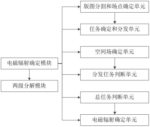
[0068] Such as figure 1 As shown, the space electromagnetic radiation calculation system provided by this embodiment mainly includes: an electromagnetic radiation determination module and a two-stage decomposition module.

[0069] The electromagnetic radiation determination module is used to convert the three-dimensional problem of electromagnetic radiation of the multilayer integrated circuit space into a sub-calculation task of the electromagnetic field generated in space by the distributed current on the simple polygon by performing two-level decomposition, and the sub-computation task is passed through the calculation unit of the GPU Fast parallel computing to realize space electromagnetic radiation calculations based on the irregular and multi-scale polygons formed by the mul...


PUM


Abstract

The present invention provides an integrated circuit-oriented space electromagnetic radiation calculation system and method. By performing two-level decomposition, the three-dimensional problem of multilayer integrated circuit space electromagnetic radiation is converted into a sub-calculation task of the electromagnetic field generated by the distributed current on a simple polygon in space. The sub-computing tasks are quickly parallelized by the computing unit of the GPU, and the irregular and multi-scale polygons formed by the layout of the multi-layer VLSI are realized. The calculation of electromagnetic radiation in space realizes the calculation of the field generated by a point current source at any position in space based on the dyadic Green's function, and uses the two-dimensional Gaussian integral method to calculate the field generated by a surface current source at the same position, and then calculates the high geometric complexity. The field generated by the current on the layout of the multilayer integrated circuit at different positions in space, based on the principle of linear superposition of the field, determines the electromagnetic radiation of the multilayer integrated circuit to the space.

Description

technical field [0001] The invention relates to the technical field of integrated circuits, in particular to an integrated circuit-oriented space electromagnetic radiation calculation system and method. Background technique [0002] Integrated circuit (integrated circuit) is a kind of miniature electronic device or component, which uses a certain process to interconnect the transistors, resistors, capacitors, inductors and other components and wiring required in a circuit, and make them in a small or several On a small semiconductor wafer or dielectric substrate, it is then packaged in a package to become a microstructure with the required circuit function. [0003] Since the integrated circuit will generate high-speed signal transmission on the multi-layer layout when it is working, it will form a high-frequency alternating electromagnetic field. These high-frequency alternating electromagnetic fields will form a high-frequency radiation source, making it harmful to other s...

Claims


Application Information

Patent Timeline
Patent Type & Authority Patents(China)
IPC IPC(8): G06F30/23G06F30/39
CPCG06F30/23G06F30/39
Inventor 唐章宏邹军汲亚飞王芬黄承清
Owner 北京智芯仿真科技有限公司
Learn More