Anti-electromagnetic interference image monitoring device
An anti-electromagnetic interference and monitoring device technology, applied in TV, color TV, image communication, etc., can solve the problems of high cost, test electromagnetic field uniform disturbance, large volume, etc., to improve data accuracy and test uniform electromagnetic field disturbance Small, small effect of electromagnetic field disturbance
- Summary
- Abstract
- Description
- Claims
- Application Information
AI Technical Summary
Problems solved by technology
Method used
Image

Examples
Embodiment 1
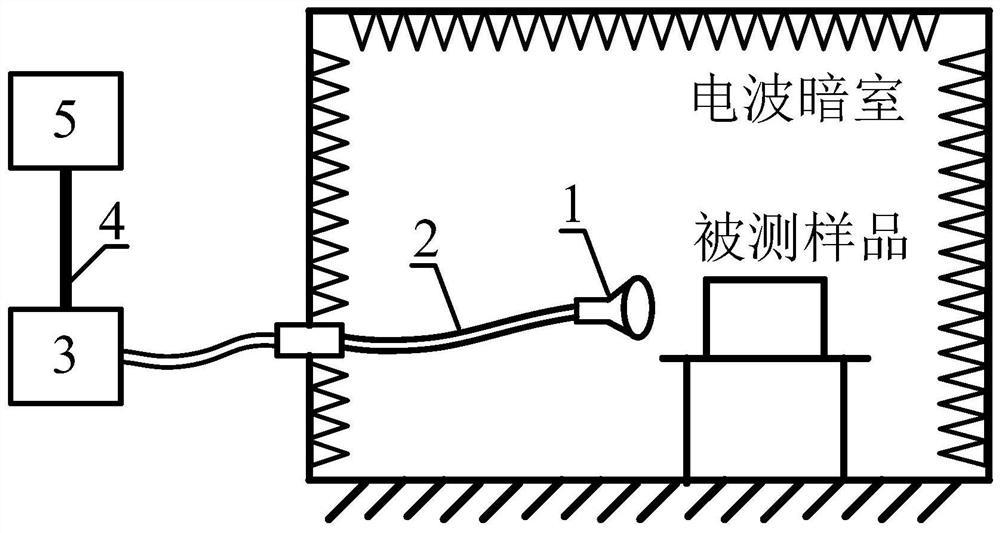
[0023] An image monitoring device with anti-electromagnetic interference disclosed in this embodiment, such as figure 1 As shown, it includes an optical imaging system 1, an image transmission fiber bundle 2 and an image analysis host 3;
[0024] The optical imaging system 1 includes an imaging lens, which is used to efficiently couple the sample to be tested into the imaging end of the image transmission fiber bundle 2;
[0025] The optical imaging system 1 is made of an integral non-metallic material, and its interior is mainly made of glass material, and its outer shell is made of plastic material, in order to avoid disturbance to the uniform electromagnetic field in the test, and to avoid the influence of strong electromagnetic interference;
[0026] The image-transmitting optical fiber bundle 2 is a commercial optical fiber bundle, and is used to transmit the image elements with different brightness on the imaging end face to the image analysis host.
[0027] Preferably,...
Embodiment 2
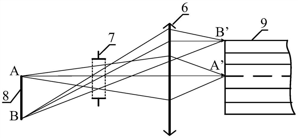
[0038] Based on the anti-electromagnetic interference image monitoring device of the first embodiment, such as figure 2 Shown is a schematic structural diagram of an embodiment of the optical imaging system 1 , which mainly includes an optical imaging lens 6 and a diaphragm 7 .
[0039] The optical imaging lens 6 images the sample 8 to be tested on the imaging end face 9 of the imaging fiber bundle 2 .
[0040] The diaphragm 7 is a traditional diaphragm structure, which can be opened or reduced to improve the quality of the image.
Embodiment 3
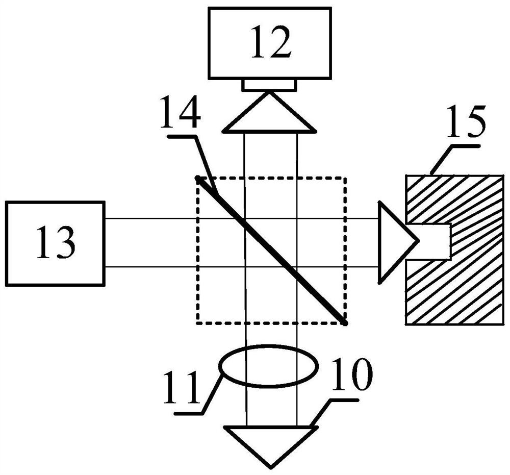
[0042] Based on the anti-electromagnetic interference image monitoring device of the first embodiment, such as image 3 Shown is a schematic structural diagram of an embodiment of the image analysis host 3 , which mainly includes a fiber bundle interface 10 , a focusing lens 11 , an image detector 12 , an illumination light source 13 , a beam splitter 14 and an optical trap 15 .
[0043] The size of the fiber bundle interface 10 should match the size of the image-transmitting fiber bundle 2 to ensure good optical coupling characteristics.
[0044] The focusing lens 11 is an optical lens group structure, which is used to solve the problem of off-axis aberration correction of the lens and the uniformity of the illuminance of the image surface, and improve the imaging quality.
[0045] The image detector 12 is a CCD image detector for receiving images.
[0046]The illumination light source 13 couples the emitted light beam into the interface 10 of the image transmission fiber bu...
PUM
 Abstract
Description
Claims
Application Information
 - R&D
- Intellectual Property
- Life Sciences
- Materials
- Tech Scout
- Unparalleled Data Quality
- Higher Quality Content
- 60% Fewer Hallucinations
Browse by: Latest US Patents, China's latest patents, Technical Efficacy Thesaurus, Application Domain, Technology Topic, Popular Technical Reports.
© 2025 PatSnap. All rights reserved.Legal|Privacy policy|Modern Slavery Act Transparency Statement|Sitemap|About US| Contact US: help@patsnap.com