Method for manufacturing long-term efficient anti-reflection micro-nano structure on copper surface and application

A technology of micro-nano structure and copper surface, used in manufacturing tools, ion implantation plating, coating, etc., can solve the problems of failure of anti-reflection effect and degradation of reflectivity, and achieves a large selection range, high-efficiency anti-reflection characteristics, long-term The effect of the high-efficiency anti-reflection feature

Active Publication Date: 2021-06-15
NORTHWESTERN POLYTECHNICAL UNIV
View PDF7 Cites 5 Cited by
  • Summary
  • Abstract
  • Description
  • Claims
  • Application Information

AI Technical Summary

Problems solved by technology

However, the problem of reflectivity degradation over time always exists: after 3-4 weeks in the air, the color of the microstructure surface changes from dark black to purple or green, which is due to the oxidation of the copper surface microstructure
In order to prevent the oxidation of the micro-nano structure on the surface, resulting in the failure of the anti-reflection effect
[0007] Through the above analysis, the existing problems and defects of the prior art are: due to the oxidation of the copper surface microstructure, the color of the microstructure surface changes from dark black to purple or green after being placed in the air for 3-4 weeks, and the reflectivity changes with time. The problem of degradation is always there

Method used


Image

  • Method for manufacturing long-term efficient anti-reflection micro-nano structure on copper surface and application
  • Method for manufacturing long-term efficient anti-reflection micro-nano structure on copper surface and application
  • Method for manufacturing long-term efficient anti-reflection micro-nano structure on copper surface and application

Examples


Embodiment 1

[0042] 1. Main structure and principle of the present invention

[0043] Schematic diagram of the preparation process of long-term anti-reflection structure on copper surface. figure 2 shown.

[0044] 2. The purpose of the invention

[0045] The purpose of the present invention is to provide a long-term high-efficiency anti-reflection micro-nano structure and its preparation method on the copper surface. The pulsed laser is used to scan the surface of the copper element, and a regular micro-nano composite structure can be prepared on the copper surface, and then inert on the surface of the micro-nano structure. Thin film growth, so that it has long-term and efficient anti-reflection function characteristics. In addition, the selection range of the processing laser in the present invention is large, which expands the scope of application.

[0046] The present invention uses nanosecond, picosecond and femtosecond lasers to prepare various micro-nano processing on the surface...

Embodiment 2

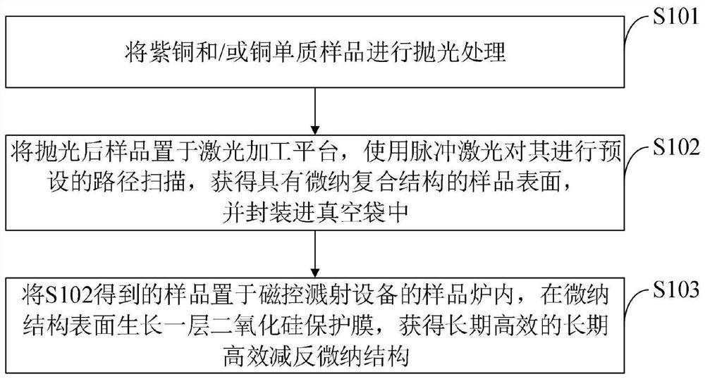
[0057] The method for manufacturing a long-term high-efficiency anti-reflection micro-nano structure on a copper surface provided by the embodiment of the present invention, the specific steps are:

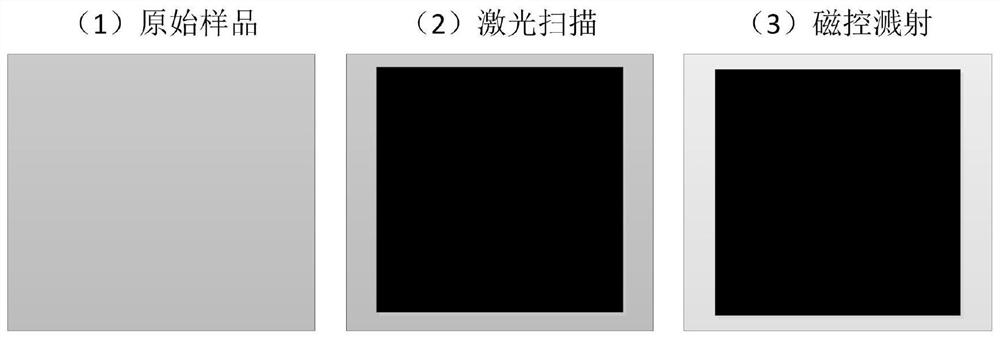
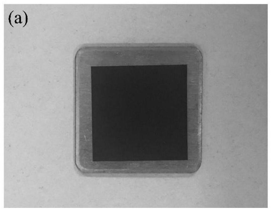
[0058] (1) Use a polishing machine to mechanically polish the surface of the copper element to obtain a processed sample.

[0059] (2) A nanosecond laser is used to scan the two-dimensional groove on the surface of the copper sample to obtain an anti-reflection micro-nano structure surface. The distance between the two-dimensional grooves is 30 μm; the parameters of the nanosecond laser are: repetition frequency 100 kHz, center wavelength 532 nm, pulse width 10 ns, and laser power 20 W.

[0060] (3) Coating a silicon dioxide protective layer on the surface of the sample obtained in step (2) by magnetron sputtering to obtain an anti-reflection micro-nano structure surface with an inert protective layer. The parameters of the magnetron sputtering are: pressure 0.5Pa, argon flow rat...

Embodiment 3

[0062] The method for manufacturing a long-term high-efficiency anti-reflection micro-nano structure on a copper surface provided by the embodiment of the present invention, the specific steps are:

[0063] (1) Use a polishing machine to mechanically polish the surface of the copper element to obtain a processed sample.

[0064] (2) Use a picosecond laser to scan the surface of the copper sample with a square grid to obtain an anti-reflection micro-nano structure surface. The side length of the square grid is 20 μm; the parameters of the picosecond laser are: repetition frequency 200 kHz, center wavelength 1030 nm, pulse width 10 ps, ​​and laser power 2000 mW.

[0065] (3) Coating a silicon dioxide protective layer on the surface of the sample obtained in step (2) by magnetron sputtering to obtain an anti-reflection micro-nano structure surface with an inert protective layer. The parameters of the magnetron sputtering are: pressure 0.5Pa, argon flow rate 38L / min, power 160W. ...


PUM

PropertyMeasurementUnit
wavelengthaaaaaaaaaa
thicknessaaaaaaaaaa

Abstract

The invention belongs to the technical field of high heat conduction media, and discloses a method for manufacturing a long-term efficient anti-reflection micro-nano structure on a copper surface. The method comprises the following steps: polishing red copper and/or a copper elementary substance sample; placing the polished sample on a laser processing platform, performing preset path scanning on the sample by using pulse laser to obtain a sample surface with a micro-nano composite structure, and packaging the sample into a vacuum bag; and placing the obtained sample in a sample furnace of magnetron sputtering equipment, and growing a layer of silicon dioxide protective film on the surface of the micro-nano structure to obtain the long-term efficient anti-reflection micro-nano structure. According to the method, the micro-nano structure with the anti-reflection characteristic is prepared on the copper surface, and then a layer of inert film is grown on the surface of the micro-nano structure for protection through a film coating method, so that the micro-nano structure has the long-term efficient anti-reflection function characteristic; and the thickness of the silicon dioxide protection layer is flexibly controlled by controlling the coating time of magnetron sputtering, the strength performance of the protection layer is improved, and the problem of failure of the anti-reflection structure on the copper surface is effectively solved.

Description

technical field [0001] The invention belongs to the technical field of high thermal conductivity media, and in particular relates to a method and application for manufacturing a long-term high-efficiency anti-reflection micro-nano structure on a copper surface. Background technique [0002] At present, copper has excellent thermal conductivity. Red copper, also known as red copper, is industrial pure copper. Its electrical conductivity and thermal conductivity are second only to precious metal silver. It is widely used in the preparation of electrical, thermal and heat dissipation devices. , LD and other power cooling devices are the most commonly used high thermal conductivity medium. [0003] However, neither copper nor copper alloys can efficiently absorb visible light, near-infrared light, and long-wave infrared light. The average reflectance of copper in the visible light band (400nm-700nm) is greater than 50%, and the average reflectance of copper from wavelength 700n...

Claims


Application Information

Patent Timeline
Patent Type & Authority Applications(China)
IPC IPC(8): B23P15/00B23K26/352C23C14/35C23C14/10
CPCB23P15/00B23K26/352C23C14/35C23C14/10
Inventor 程光华娄睿张国栋王江
Owner NORTHWESTERN POLYTECHNICAL UNIV
Why Eureka
Try Eureka