
A method of electroplating conductive material on a semiconductor wafer

A semiconductor and conductive coating technology, applied in semiconductor devices, circuits, sputtering and other directions, can solve the problem of uneven thickness of the coating, and achieve the effect of fast preparation, not easy to crack, and high processing ability index

Active Publication Date: 2022-05-13
WUXI WELNEW MICRO ELECTRONICS
View PDF0 Cites 0 Cited by
  • Summary
  • Abstract
  • Description
  • Claims
  • Application Information

AI Technical Summary

Problems solved by technology

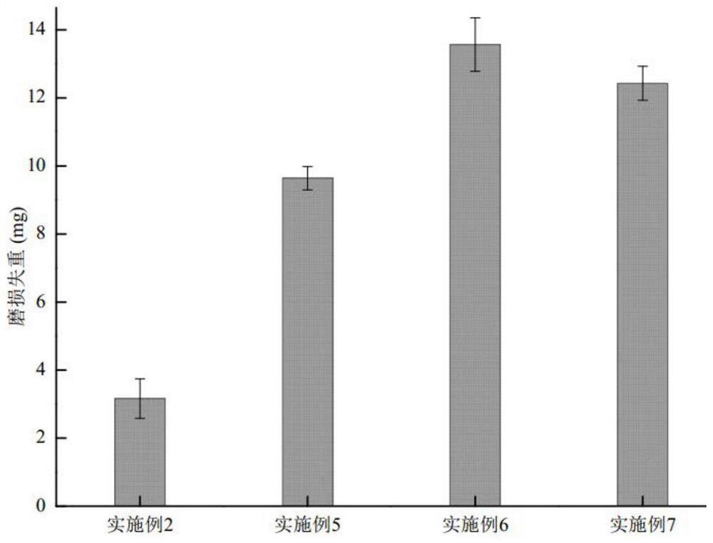
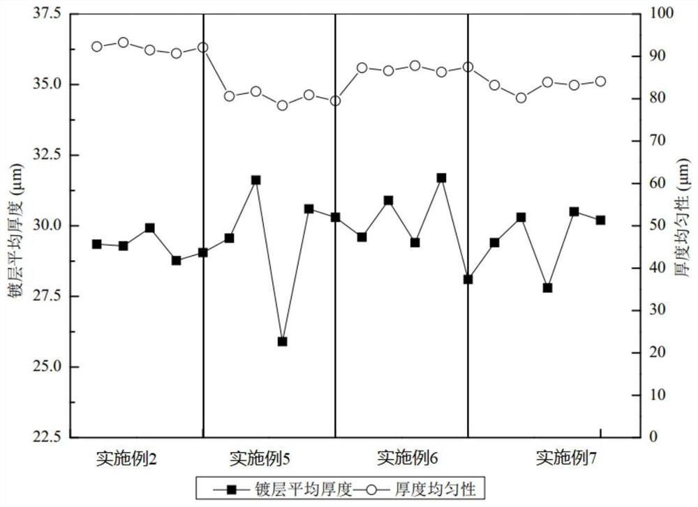
[0005] The purpose of the present invention is to provide a method that overcomes the lack of uneven coating thickness in the prior art, can improve the dispersion ability of the plating solution, improve the thickness uniformity and hardness of the electroplated silver coating, enhance the anti-tarnish ability and wear resistance of the coating, and gain electrical conductivity. A method for electroplating conductive materials on semiconductor wafers with high performance and extended mechanical life and high process capability index

Method used


Image

  • A method of electroplating conductive material on a semiconductor wafer
  • A method of electroplating conductive material on a semiconductor wafer
  • A method of electroplating conductive material on a semiconductor wafer

Examples


Embodiment 1

[0043] A method for electroplating conductive material on a semiconductor wafer, comprising the following steps:

[0044] 1) Fix the cleaned wafer in the inner chamber, and then place the three materials of titanium, nickel and silver with a purity of more than 99.99% respectively in three acupuncture points on the rotating workpiece disk of the evaporation table;

[0045] 2) Close and seal the inner chamber, and then start the vacuum system to evacuate the inner chamber to 1.0×10 -4 Pa;

[0046] 3) First put the acupuncture point containing the titanium material at the working position, start the evaporation source and power on, adjust the current to 100A, open the baffle to start evaporation, the titanium material is heated to the boiling point and evaporated, depositing a layer of titanium on the surface of the wafer coating, when the preset thickness is reached, switch the acupuncture point on the evaporation source, use the same operation and sequentially vapor-deposit n...

Embodiment 2

[0059] A method for electroplating conductive material on a semiconductor wafer, when working, differs from Embodiment 1 only in that:

[0060] Step 5), the degreasing conditions are: the concentration of potassium hydroxide solution is 150g / L, and the degreasing temperature is 50°C;

[0061] Step 6), the concentration of potassium citrate solution for activation is 50mL / L;

[0062] Step 7), the silver plating conditions are: at a stirring rate of 650rpm, a liquid temperature of 20°C, and a current density of 1.0A / dm 2 Electroplating under the conditions of 15min, after forming a silver coating with a thickness of 25-35μm, the above electroplating solution includes: 7g / L potassium hydroxide, 25g / L silver potassium cyanide, 15mL / L dimethylhydantoin, 80g / L of potassium carbonate, 15g / L of nonylphenol polyoxyethylene ether, 3.5g / L of additives, deionized water as solvent; pH is 7.8; the solvent of the above additives is absolute ethanol, which also has 7g The 2-carboxy-5-fluoro...

Embodiment 3

[0068] A method for electroplating conductive material on a semiconductor wafer, when working, differs from Embodiment 1 only in that:

[0069] Step 5), the degreasing conditions are: the concentration of potassium hydroxide solution is 100g / L, and the degreasing temperature is 40°C;

[0070] Step 6), the concentration of potassium citrate solution for activation is 30mL / L;

[0071] Step 7), the silver plating conditions are: the stirring rate is 600rpm, the liquid temperature is 10°C, and the current density is 0.5A / dm 2 Electroplating under the conditions of 15min, after forming a silver coating with a thickness of 25-35μm, the above electroplating solution includes: 5g / L potassium hydroxide, 20g / L silver potassium cyanide, 10mL / L dimethylhydantoin, Potassium carbonate of 70g / L, nonylphenol polyoxyethylene ether of 10g / L, additive of 1.5g / L, deionized water is solvent; pH is 7.8; The solvent of above-mentioned additive is absolute ethanol, and 9g The sodium bismuth titanat...


PUM

PropertyMeasurementUnit
thicknessaaaaaaaaaa
thicknessaaaaaaaaaa
thicknessaaaaaaaaaa

Abstract

The invention provides a method for electroplating a conductive material on a semiconductor wafer, which relates to the technical field of semiconductor manufacturing technology, including forming a conductive coating on a wafer substrate; the conductive coating includes an electroplated silver coating on the surface, and the electroplating silver coating and the wafer Titanium-nickel-silver coating between substrates; the above-mentioned nickel-titanium-silver coating is prepared by vacuum evaporation technology, and the electroplated silver coating is prepared by rack plating technology; the thickness of the above-mentioned nickel-titanium-silver coating is 2.1-3.5 μm, and the thickness of the electroplated silver coating is 25 -35 μm. The method for electroplating conductive materials provided by the invention overcomes the deficiency of uneven coating thickness in the prior art, can improve the dispersion ability of the plating solution, improve the thickness uniformity and hardness of the electroplated silver coating, enhance the anti-discoloration ability and wear resistance of the coating, and gain Conductivity and extended mechanical life, high processing capability index; conductive materials can also include but not limited to gold, copper, zinc, chromium, rare metals (such as palladium, rhodium, etc.) in actual production.

Description

technical field [0001] The invention belongs to the technical field of semiconductor manufacturing technology, and in particular relates to a method for electroplating conductive materials on semiconductor wafers. Background technique [0002] Wafer (Wafer) refers to the silicon chip used in the production of silicon semiconductor integrated circuits. Because of its circular shape, it is called a wafer. It can be processed into various circuit element structures on silicon wafers, and become IC products with specific electrical functions. IC products are the basic original devices that are inseparable from the modern information society, and are widely used in all aspects of our lives. [0003] Electroplating is a process of plating a thin layer of conductive materials such as metal or alloy on the surface of a material by electrolysis. It can design and manufacture extremely thin and excellent coatings, so it is widely used in the coating process of semiconductor manufactu...

Claims


Application Information

Patent Timeline
Patent Type & Authority Patents(China)
IPC IPC(8): C25D7/12C25D3/46C23C14/24C23C14/16C23C28/02C25D5/00C25D5/08C25D5/48C25F1/00
CPCC25D7/12C25D3/46C23C14/24C23C14/16C23C28/023C25D5/00C25F1/00C25D5/48C25D5/08
Inventor 肖笛
Owner WUXI WELNEW MICRO ELECTRONICS
Learn More