
Graphical secondary development method of EDA software in chip design

A technology for chip design and secondary development, applied in CAD circuit design, computer-aided design, visual/graphic programming, etc., to achieve the effects of improving flexibility, facilitating debugging and correction, and improving debugging efficiency and accuracy

Active Publication Date: 2021-06-18
SUZHOU BATELAB MICROELECTRONICS
View PDF3 Cites 2 Cited by
  • Summary
  • Abstract
  • Description
  • Claims
  • Application Information

AI Technical Summary

Problems solved by technology

[0005] In order to overcome the above-mentioned deficiencies in the prior art, the purpose of the present invention is to propose a graphical secondary development method of EDA software in chip design, to solve the problems of easy-to-handle operation and optimized efficiency of the software

Method used


Image

  • Graphical secondary development method of EDA software in chip design
  • Graphical secondary development method of EDA software in chip design

Examples


Embodiment Construction

[0020] The specific implementation of the present invention will be described in further detail below in conjunction with the accompanying drawings of the embodiments, so as to make the technical solution of the present invention easier to understand and grasp, so as to define the protection scope of the present invention more clearly.

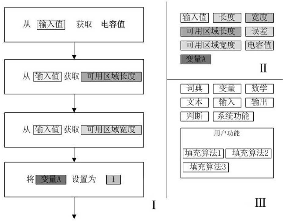
[0021] Aiming at many existing deficiencies, the designer of the present invention relies on long-term experience in chip design such as analog integrated circuits, and innovatively proposes a graphical secondary development method of EDA software in chip design, which is vivid, specific, visualized and The logical graphic editing method replaces the simple text input and editing in the past, and solves the problem of easy-to-use operation and optimized efficiency of chip layout design.

[0022] The above-mentioned graphical secondary development method of the present invention is implemented based on the system function call provided in advanc...


PUM


Abstract

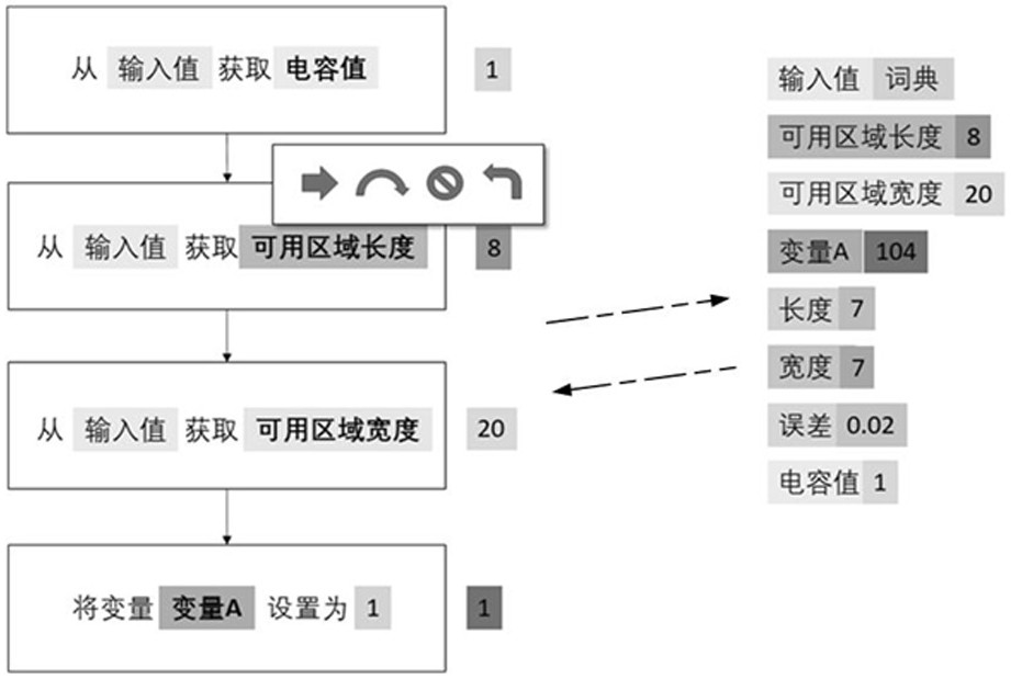
The invention discloses a graphical secondary development method of EDA (Electronic Design Automation) software in chip design. The method comprises the following steps of: converting a to-be-edited program of a text type in a chip design process into association among a plurality of nodes, patterning the association into a flow chart, and containing regions where a flow chart drawing interface, a program candidate variable and a program candidate function module are respectively located under a visual interface of a computer; a developer updates the flow chart by calling a function module to add new nodes, and assigns the nodes through variables until the flow chart is complete; a flow chart and all variables in the flow chart are presented in different regions under a visual interface of a computer, a group of input is given to the flow chart, an output result is displayed in real time, a node which causes a gap relative to an expected target is analyzed, and the output result approaches the expected target by adjusting variable assignment of part of nodes. According to the method, the operation complexity of chip layout design is reduced, the design efficiency is improved, an interactive interface is visual and friendly, and debugging is easy and convenient.

Description

technical field [0001] The invention relates to the field of semiconductor chip design, in particular to a technical solution for computer-aided chip layout design and graphic secondary development of existing EDA software. Background technique [0002] With the rapid development of smart terminal equipment, everything from small data adapters and Bluetooth headsets to large control systems for cars, ships, and airplanes cannot do without high-precision designed and processed semiconductor chips. Over the years, computer software technology has also made great breakthroughs. Among them, almost all EDA software supports secondary development as automatic devices to accelerate chip layout design. [0003] In a common development case, it is known that the capacitance value of 1μm×1μm is 0.02pF under a specific process. In order to obtain a capacitor of 1pF, the developer can manually draw a capacitor of 4μm×25μm, or draw a capacitor of 7μm×7μm capacitance (with a 2% error). ...

Claims


Application Information

Patent Timeline
Patent Type & Authority Applications(China)
IPC IPC(8): G06F8/34G06F30/31G06F30/392G06F117/08
CPCG06F8/34G06F30/31G06F30/392G06F2117/08
Inventor 李真
Owner SUZHOU BATELAB MICROELECTRONICS
Learn More