Film uncovering method

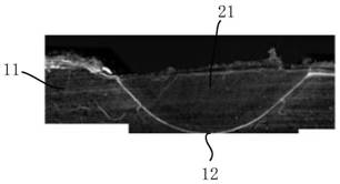
A film stripping and base film technology, which is applied in the manufacturing of electrical components, electric solid-state devices, semiconductor/solid-state devices, etc., can solve the problems of protective film 3 wrinkles, film peeling failure, affecting chip quality, etc., and achieves film peeling safety and reliability. Good reliability, avoids the risk of damage, and extends the effect of the range of use

Pending Publication Date: 2021-06-22
SEMICON MFG ELECTRONICS (SHAOXING) CORP
View PDF6 Cites 0 Cited by
  • Summary
  • Abstract
  • Description
  • Claims
  • Application Information

AI Technical Summary

Problems solved by technology

[0004] The above thermocompression bonding process usually requires that the protective film 3 has the characteristics of high temperature resistance and high pressure resistance, but the protective film 3 with this characteristic is relatively hard, and the buffer protection effect is poor, which is likely to cause damage to the functional surface of the wafer and affect the quality of the chip.
However, if a protective film 3 that does not have high temperature resistance and high pressure resistance is selected for use, after thermal compression bonding, if Figure 3a As shown, the residue 31 (ie residual glue) of the protective film 3 will be left on the surface of the wafer 4, and the residue 31 will cause the risk of contamination and debris during subsequent wafer processing.
If the thermocompression process is not used, then if Figure 3b As shown, it is easy to cause wrinkles 32 in the protective film 3, resulting in the failure of peeling off the film.

Method used


Image

  • Film uncovering method
  • Film uncovering method
  • Film uncovering method

Examples


Embodiment Construction

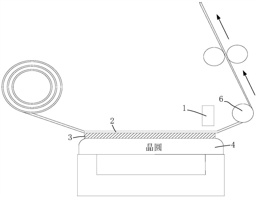
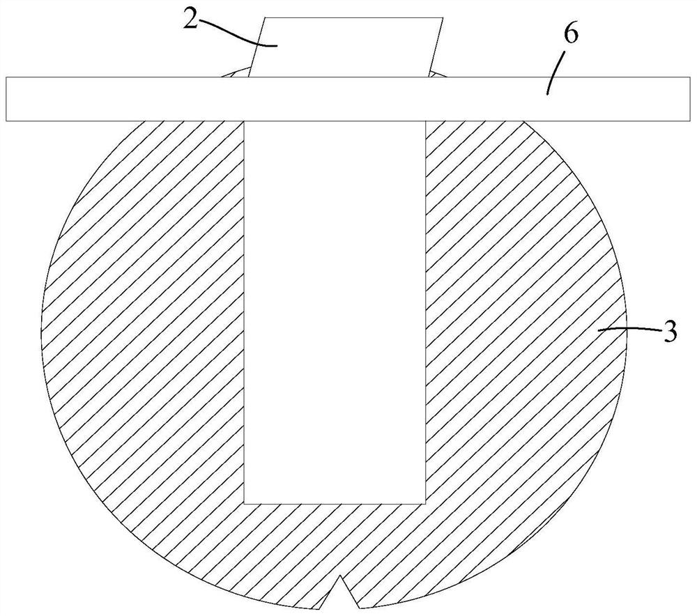
[0040] In describing the present invention, it should be understood that the terms "length", "width", "upper", "lower", "front", "rear", "left", "right", "vertical", The orientations or positional relationships indicated by "horizontal", "top", "bottom", "inner", "outer", etc. are based on the orientation or positional relationships shown in the drawings, and are only for the convenience of describing the present invention and simplifying the description, and It is not to indicate or imply that the device or element referred to must have a particular orientation, be constructed in a particular orientation, or operate in a particular orientation, and thus should not be construed as limiting the invention. In the description of the present invention, the term "edge" refers to the peripheral portion of the substrate, ie to the portion along the edge.

[0041] In the description of the present invention, "plurality" means two or more, unless otherwise specifically defined. In the...


PUM

PropertyMeasurementUnit
thicknessaaaaaaaaaa
thicknessaaaaaaaaaa
thicknessaaaaaaaaaa

Abstract

The invention relates to a film uncovering method which comprises the following steps: providing a substrate to which a protective adhesive tape is attached, forming a notch at the edge of the substrate, and enabling the protective adhesive tape to completely coincide with the notch; pressing the film uncovering adhesive tape on the protective adhesive tape in a non-thermal pressing manner; and using the film stripping mechanism for tearing the film uncovering adhesive tape from the notch position, and removing the protective adhesive tape from the substrate. Under the conditions of no heating and no auxiliary device, the protective adhesive tape is successfully removed from the substrate, the protective adhesive tape made of a soft material is conveniently selected to protect the substrate, the risk of damage to the substrate in the processing process is avoided, the product quality is ensured, and the film uncovering cost is reduced.

Description

technical field [0001] The invention relates to the technical field of semiconductors, in particular to a method for peeling off a film. Background technique [0002] In the semiconductor device manufacturing process, after forming many semiconductor devices on the functional surface of the wafer, the wafer back grinding process (Back Grinding tape, referred to as BG) is performed, and the wafer is ground to correspond to the functional surface by a planarization process. Part of the thickness of the wafer is removed from the backside of the wafer to reduce the thickness of the subsequently formed chip. In the process of grinding the back of the wafer, a layer of protective tape (BG tape) will be covered on the functional surface of the wafer first to avoid contamination of the functional surface of the wafer caused by impurities generated during the process of grinding the back of the wafer, and to avoid The functional surface of the wafer is directly in contact with the g...

Claims


Application Information

Patent Timeline
Patent Type & Authority Applications(China)
IPC IPC(8): H01L21/683
CPCH01L21/6836H01L2221/68327H01L2221/6834H01L2221/68386
Inventor 黄阳王友铸
Owner SEMICON MFG ELECTRONICS (SHAOXING) CORP
Why Eureka
Try Eureka