Preparation method of three-dimensional memory

A memory, three-dimensional technology, applied in the direction of semiconductor devices, electrical solid devices, electrical components, etc., can solve the problems of silicon groove opening damage, difficulty in drilling, and inability to form silicon grooves, so as to prevent leakage current and ensure etching effect of effect

Active Publication Date: 2022-06-03
YANGTZE MEMORY TECH CO LTD
View PDF8 Cites 0 Cited by
  • Summary
  • Abstract
  • Description
  • Claims
  • Application Information

AI Technical Summary

Problems solved by technology

The increased thickness of the deposited layer and the smaller critical dimensions lead to the side-capping of the bottom of the gate layer after the deposition process, resulting in tungsten residue after etch
Residual tungsten may affect the threshold voltage of the bottom selection gate and cause leakage current, and the residual tungsten also prevents the formation of silicon grooves during sidewall etching, which affects the final electrical performance
[0004] In the prior art, when the metal tungsten layer is directly etched by wet etching, the width of the bottom and top of the metal tungsten in the channel after etching is not uniform, that is, the RECESS GAP is very large, unable to meet production requirements
However, when dry etching is used to etch the metal tungsten layer, due to the anisotropy of dry etching, the metal tungsten deposited on the bottom sidewall of the gate line gap cannot be completely removed.
At this time, it is usually necessary to increase the intensity of dry etching to remove tungsten residues. However, too strong dry etching will cause the opening of the silicon groove to be damaged and enlarged, which will cause the oxidation of the opening at the subsequent filling of silicon oxide. Silicon layer is too thick
An overly thick silicon oxide layer will make it difficult to drill holes in the subsequent process that requires opening holes for circuit outreach.

Method used


Image

  • Preparation method of three-dimensional memory
  • Preparation method of three-dimensional memory
  • Preparation method of three-dimensional memory

Examples


preparation example Construction

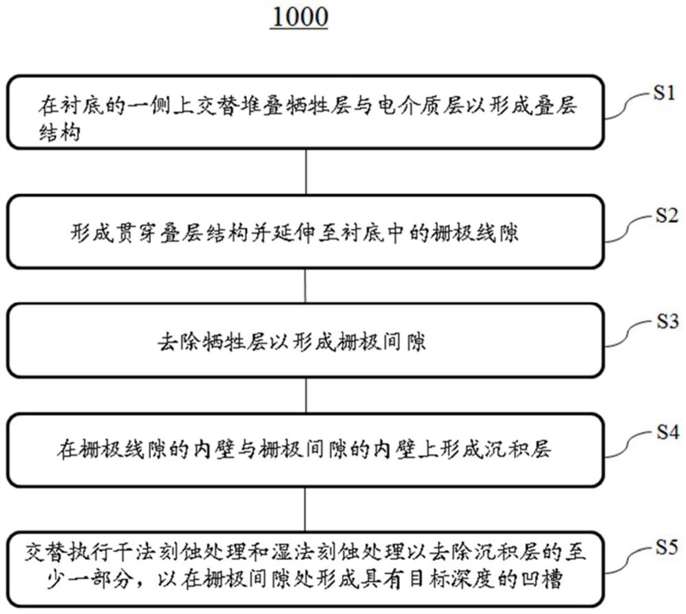
[0039] FIG. 1 is a flowchart of a method 1000 for fabricating a three-dimensional memory according to an exemplary embodiment of the present application. like

[0040] S1, alternately stacking sacrificial layers and dielectric layers on one side of the substrate to form a stacked structure.

[0041] S2, forming a gate line gap extending through the stacked structure and extending into the substrate.

[0042] S3, removing the sacrificial layer to form a gate gap.

[0043] S4, forming a deposition layer on the inner wall of the gate line gap and the inner wall of the gate gap.

[0045] The specific process of each step of the above-mentioned preparation method 1000 will be described in detail below. For ease of understanding, the following

[0046] In step S1, the dielectric layers and the sacrificial layers are alternately stacked on the substrate 100 to form a stacked structure, which may include:

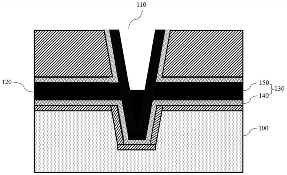
[0047] In step S2, a gate line gap 110 extending through the stacked structure an...

Embodiment approach

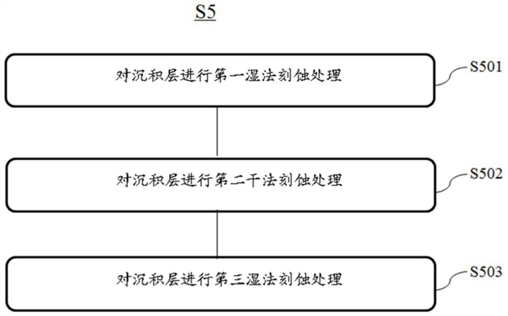
[0054] In step S501, a portion of the metal layer 150 deposited on the inner wall of the gate line gap 110 and the gate gap 120 may be

[0055] According to an exemplary embodiment, when the metal layer 150 is a tungsten layer, wet etching (eg, by high

[0056] In step S502, the remaining metal layer 150 and the barrier layer 140 on the bottom of the gate line gap 110 may be subjected to a first step.


PUM

PropertyMeasurementUnit
depthaaaaaaaaaa

Abstract

The present application provides a method for preparing a three-dimensional memory, the method comprising: alternately stacking sacrificial layers and dielectric layers on one side of a substrate to form a stacked structure; a gate line gap; removing the sacrificial layer to form a gate gap; forming a deposition layer on an inner wall of the gate line gap and an inner wall of the gate gap; and alternately performing a dry etching process and a wet etching process to remove the deposition layer At least a portion of the gate gap to form a groove having a target depth at the gate gap.

Description

Preparation method of three-dimensional memory technical field [0001] The present application relates to the field of semiconductor manufacturing, and more particularly, to a method for preparing a three-dimensional memory. Background technique [0002] To overcome the limitations of two-dimensional (2D) memory devices, three-dimensional (3D) arrangement of memory cells on a substrate is currently to increase the integration density. Existing 3D NAND memory architectures typically have gate gaps arranged vertically and horizontally arranged Design of the metal gate layer. Common fabrication processes for 3D NAND memory include: forming a gate structure between insulating layers, Wherein, the gate structure sequentially includes a barrier layer and a metal tungsten layer from the inside to the outside; then the metal tungsten layer is etched to obtain a metal gate Floor. For example, the metal tungsten layer may be etched using wet etching or dry etching. [0003] Th...

Claims


Application Information

Patent Timeline
Patent Type & Authority Patents(China)
IPC IPC(8): H01L21/28H01L27/11524H01L27/11551H01L27/1157H01L27/11578
CPCH01L29/401H10B41/20H10B41/35H10B43/20H10B43/35
Inventor 刘力恒长江徐伟许波
Owner YANGTZE MEMORY TECH CO LTD
Why Eureka
Try Eureka