Wafer laser slicing device with good effect

A slicing device and wafer technology, applied in laser welding equipment, welding equipment, metal processing equipment, etc., can solve the problems of affecting the aesthetics of the workpiece, scratching the surface of the workpiece, and large energy consumption, so as to improve stability and service life , improve efficiency and save energy

Inactive Publication Date: 2021-06-29
南京依扬知识产权代理有限公司
View PDF0 Cites 0 Cited by
  • Summary
  • Abstract
  • Description
  • Claims
  • Application Information

AI Technical Summary

Problems solved by technology

[0003] Wafers generally use a cutting device to slice and shape silicon ingots. However, the existing wafer slicing devices generally require multiple driving sources to drive the pushing of the workpiece and the movement of the cutting mechanism, which consumes a lot of energy. At the same time, the existing The slicing device generally adopts rigid clamping for the workpiece. Rigid clamping is easy to scratch the surface of the workpiece, affecting the aesthetics of the workpiece, and even causing damage to the workpiece.

Method used


Image

  • Wafer laser slicing device with good effect
  • Wafer laser slicing device with good effect
  • Wafer laser slicing device with good effect

Examples


Embodiment Construction

[0026] The present invention is described in further detail now in conjunction with accompanying drawing. These drawings are all simplified schematic diagrams, which only illustrate the basic structure of the present invention in a schematic manner, so they only show the configurations related to the present invention.

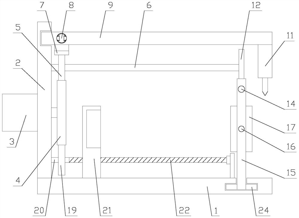
[0027] Such as figure 1 As shown, a wafer laser slicing device with good effect includes a base 1, a support rod 2, a driving mechanism, a slicing mechanism, a clamping mechanism and a pushing mechanism. The support rod 2 is arranged at one end of the base 1, and the The driving mechanism is arranged on the pole 2, the clamping and pushing mechanism is arranged on the base 1, the slicing mechanism is arranged on the pole 2, and the clamping mechanism is arranged above the base 1;

[0028] When the device is in use, the workpiece is clamped by the clamping mechanism, the driving mechanism is operated, and the driving mechanism drives the pushing mechanism to m...


PUM


Abstract

The invention relates to a wafer laser slicing device with a good effect. The wafer laser slicing device comprises a base, a supporting rod, a driving mechanism, a slicing mechanism, a clamping mechanism and a pushing mechanism; according to the wafer laser slicing device, a workpiece is clamped through the clamping mechanism; the driving mechanism is operated; the driving mechanism drives the slicing mechanism and the pushing mechanism to intermittently operate; and therefore the workpiece is sliced. Compared with an existing clamping mechanism, the clamping mechanism flexibly clamps workpieces; the situation that the workpieces are scratched through rigid clamping is avoided; the workpieces are protected; compared with an existing slicing device, the device achieves pushing of the workpieces and movement of a laser cutter through one output end; energy is saved; meanwhile, the slicing mechanism and the pushing mechanism are linked; online pushing and slicing of the workpieces are achieved; efficiency is improved; the linkage is of a pure mechanical structure; use of electronic elements such as a sensor is avoided; the stability of the device is improved; and the service life of the device is prolonged.

Description

technical field [0001] The invention relates to a wafer laser slicing device with good effect. Background technique [0002] Wafer refers to the silicon wafer used in the production of silicon semiconductor integrated circuits. Because of its circular shape, it is called a wafer. It can be processed into various circuit element structures on the silicon wafer and become an IC with specific electrical functions. product. The raw material of the wafer is silicon, and the surface of the earth's crust has an inexhaustible amount of silicon dioxide. Silica ore is refined by electric arc furnace, chlorinated by hydrochloric acid, and distilled to produce high-purity polysilicon wafers. , made high-purity polysilicon, and the wafer manufacturing plant melted the polysilicon, and then planted a seed crystal in the melt, and then slowly pulled it out to form a cylindrical single crystal silicon rod, silicon crystal The bars need to be sectioned, tumbled, sliced, chamfered, polishe...

Claims


Application Information

Patent Timeline
Patent Type & Authority Applications(China)
IPC IPC(8): B23K26/08B23K26/38B23K26/402B23K26/70
CPCB23K26/08B23K26/38B23K26/402B23K26/702
Inventor 黄娉
Owner 南京依扬知识产权代理有限公司
Why Eureka
Try Eureka