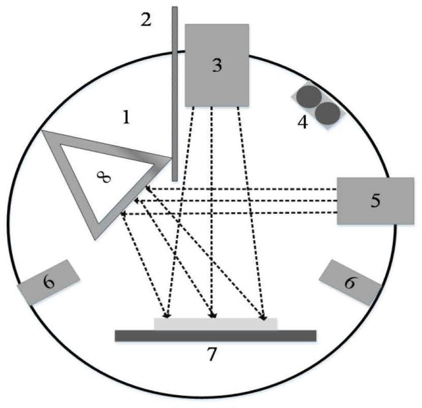
[0021] In order to make the objects and advantages of the present invention, the present invention will be described in further detail below with reference to the embodiments. It will be appreciated that the specific embodiments described herein are merely illustrative of the invention and are not intended to limit the invention. During the growth of the film, the generation of film stress is inevitable. Film stress is usually divided into tensile stress and pressure stress. Usually, the obtained film prepared by the method of bispeling sputtering is highly compressive stress. The offline calculation method of film stress is as follows. Attach figure 1 It is the relationship between the diameter of the substrate, the height, and the radius of curvature, and the radius control schematic diagram of the curvature radius. Attach figure 1 (a), the relationship between the substrate diameter, the height, and the radius of curvature can be expressed as:
[0022]
[0023] Where R is the radius of curvature, D s For the substrate diameter, H is rising.
[0024] The relationship between the Height and Power is:
[0025] H = 2 × 632.8 × power (2)
[0026] Usually, the substrate caused by the film stress is small, so the relationship between Power and the radius R R is approximately:
[0027]
[0028] Where DS is the diameter of the circular substrate.
[0029] Can be further obtained:
[0030]
[0031] This definition ΔPower is before and after the coating (Power 2 , Power 1 ) The difference between the surface precision Power, R 0 R 1 The radius of curvature of the substrate before and after the coating is respectively. Therefore, the relationship between the change in surface precision and the film stress can also be written as:
[0032]
[0033] t f For the film layer thickness, it can be obtained according to the transmittance spectrum. t s T f The thickness of the substrate and film, e s And V s Elastic modulus and Poisson ratio of the substrate (reference [1]: S.W.deng, F.Wang, S.Liu, Residualstress Prediction and Control of Ta 2 O 5 / Sio 2 Multilayer based on layer.Tructure Designing, chin.opt.lett.11 (2013) 10701.), σ is the film stress.
[0034] After the film stress is generated, the substrate will cause curved deformation. According to the formula (4), we know the relationship between ΔPower and the radius of curvature, that is, after the plating film, due to the presence of stress, the amount of change in the radius of curvature of the substrate can be calculated by measuring the amount of curvature. The radius target value of the curvature is reversed (5) can calculate how much change is calculated to produce a substrate POWER value. The thickness of the film can be obtained according to the relationship between the thickness of the film and the amount of wavelength of the wave. Finally realize the precise control of the radius of curvature of the large curvature substrate. figure 1 (b) is a schematic diagram of the radius of curvature of the optical element of the large curvature. After optical processing, as shown, when the radius of curvature is smaller than the target value, a layer of corresponding thickness is plated in the rear surface of the substrate. 2 The film can be controlled by the radius of curvature. When the radius of curvature is larger than the target value, a layer of corresponding thickness is plated on the front surface of the substrate. 2 The film can be controlled by the radius of curvature. However, plating SIO in front surface 2 The film can affect the spectral characteristics of the film, so the front surface plating SIO 2 The film method is only suitable for the preparation of the high reaction.
[0035] Specific embodiment of the invention: The parameters of the large curvature radius optical element to be processed are: the radius of curvature r = 35.7m.
[0036] use equipment:
[0037] The film samples of this experiment are prepared on a double ion beam sputtering deposition system, and the experimental device is attached. figure 2 As shown, the vacuum chamber has 16CMRF main ionosphere and a 12 cmRF auxiliary ion source, and the ion source has a radio frequency frequency of 13.56 MHz. The sputtering target is a metal hafnium target, and when the plating film is deposited, the metal hafnium is reacted with the through-in-oxygen to obtain a cerium oxide film.
[0038] Specific process parameters:
[0039] Table 1
[0040]
[0041] First, the hair blanks of quartz are first, and the center of consciousness is the specific specification.
[0042] The optical element to be processed is polished in a process of coarse grinding, fine mill; then design and processing the curvature specular in accordance with the large curvature radius optical element structural parameters, and the radius of curvature is corrected by the abrasive correction element.
[0043] The optical element is then applied using traditional processing or CNC machining methods, and the thick polishing is guided using the test facade accuracy error.
[0044]When the optical element passes through the coarse polishing process, the radius of curvature is carried out by using the LUPHOSCAN high-speed non-contact 3D aspherical optical surface precision non-contact 3D aspherical optical surface accuracy measurement system of the British Taylor Hepson, and the radius of curvature is measured. The radius of the target curvature is 35.65m, continued using traditional processing or CNC machining methods, and its efficiency will be significantly reduced. Therefore, the method of further accurately controlling the radius of curvature of the optical element will be further accurately controlled using the invention.
[0045] The specific calculation process is as follows:
[0046] First calculate the radius of curvature of the optical element after processing polish The radius of curvature of the target target Difference ΔR = r target -R polish = 1.13m.
[0047] Put R 0 R 1 After substituting formula (1) and (2), ΔPower = 0.512 λ, λ is the main detection light wavelength, and this example corresponds to 632.8 nm.
[0048] Then on the experimental substrate (specification is The plated five groups of different thicknesses monolayers, preferably having a film thickness of 0.5 μm, 5 μm, 10 μm, 20 μm, and 30 μm, and measuring the surface precision of the substrate after the coating, the five sets of data is linearly regained, that is, the base The corresponding relationship between the change in sheet-shaped accuracy and the thickness of the film, such as Figure 4 Indicated. The specific relationship is:
[0049] Power = -0.26562-1.58224 × 10 -4 t f (6)
[0050] Continue to rewrite the formula (5) as:
[0051] σT f = C s K s Δpower (7)
[0052] among them
[0053]
[0054] Where C s It is a constant item, depending on the substrate material.
[0055]
[0056] Among them, K s It is a shape factor, depending on the ratio of the diameter of the substrate and the thickness, calculated, wherein the shape factors of the large curvature quartz substrate and the experimental substrate are 1089 and 645.16, respectively.
[0057] Finally, the required film thickness was calculated from equation (6) and (7) to 2.7 μm.
[0058] Put the quartz film after drying and drying the equipment vacuum chamber, vacuuming to <8 × 10- 2 Torr, high valve, heating tube, stable temperature at 80 ° C, vacuum to 5 × 10- 6 Torr starts depositing SIO 2 Thin film, specific parameters are shown in Table 1. After the film is completed, the test results are attached. Figure 5 As shown, it can be seen from the figure that the radius of curvature of the optical element after the stress control is 34.52 mm to 35.66 mm.
[0059] From attachment Figure 4 The contrast can be seen that embodiments of the present invention solve the problems present in the prior art and obtain a significant technical effect.