
Display panel, preparation method of display panel and display device

A display panel and touch display technology, which is applied in semiconductor/solid-state device manufacturing, data processing input/output process, instruments, etc., can solve problems such as short circuit in the terminal area, and achieve the effect of improving short circuit and reducing height

Active Publication Date: 2021-07-02
WUHAN CHINA STAR OPTOELECTRONICS SEMICON DISPLAY TECH CO LTD
View PDF9 Cites 0 Cited by
  • Summary
  • Abstract
  • Description
  • Claims
  • Application Information

AI Technical Summary

Problems solved by technology

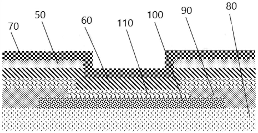
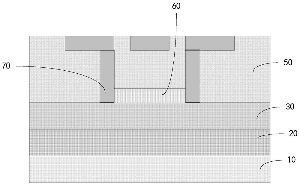
[0006] Embodiments of the present invention provide a display panel, a method for preparing a display panel, and a display device, which can effectively solve the problem of using two layers of mutual capacitive touch display panels. Metal, the problem that the terminal area is prone to short circuit caused by the layered structure of the terminal area is too high

Method used


Image

  • Display panel, preparation method of display panel and display device
  • Display panel, preparation method of display panel and display device
  • Display panel, preparation method of display panel and display device

Examples


Embodiment Construction

[0023] The following will clearly and completely describe the technical solutions in the embodiments of the present invention with reference to the drawings in the embodiments of the present invention. Apparently, the described embodiments are only some of the embodiments of the present invention, but not all of them. Based on the embodiments of the present invention, all other embodiments obtained by those skilled in the art without creative efforts fall within the protection scope of the present invention.

[0024] In the description of the present invention, it should be noted that unless otherwise specified and limited, the terms "installation", "connection" and "connection" should be understood in a broad sense, for example, it can be a fixed connection or a detachable connection. Connected, or integrally connected; it can be mechanically connected, or electrically connected, or can communicate with each other; it can be directly connected, or indirectly connected through...


PUM

PropertyMeasurementUnit
thicknessaaaaaaaaaa
thicknessaaaaaaaaaa
thicknessaaaaaaaaaa

Abstract

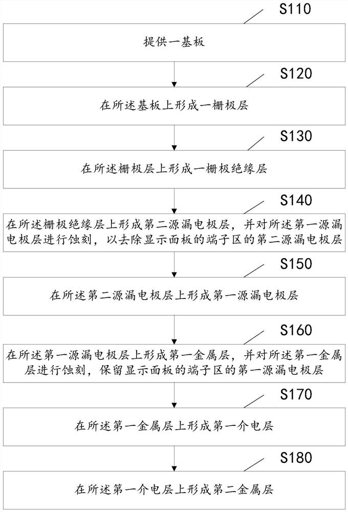
The invention discloses a display panel, a preparation method of the display panel and a display device. The display panel includes a gate layer; a gate insulating layer which is partially arranged on the gate layer; a first source and drain electrode layer which is arranged on the grid electrode layer and the grid electrode insulating layer; a first metal layer which is arranged on the first source and drain electrode layer; a first dielectric layer which is arranged on the first metal layer; and a second metal layer disposed on the first dielectric layer. Compared with the prior art, a second dielectric layer is not additionally arranged, so that the first metal layer is directly deposited on the thin film packaging layer, and meanwhile, the first metal layer is reserved in the terminal area, so that the problem of side etching of the first source and drain electrode layer in the terminal area can be solved; meanwhile, the second source and drain electrode layer in the terminal area is removed to reduce the height of the terminal area, so that the problem that short circuit possibly occurs in the terminal area is solved.

Description

technical field [0001] The invention relates to display panel technology, in particular to a display panel, a method for preparing the display panel and a display device. Background technique [0002] Display devices mainly include liquid crystal display (LCD for short), plasma display panel (PDP for short), organic light emitting diode (OLED for short), active matrix organic electroluminescence (Active Matrix organic light emitting diode, referred to as AMOLED), has a broad application space in vehicles, mobile phones, tablets, computers and TV products. [0003] OLED screens have the characteristics of thinness, high contrast, flexibility, and high transmittance, and have begun to become the mainstream screens of high-end smartphones. Technologies such as under-screen fingerprints, under-screen cameras, and under-screen sound have also been developed one after another. [0004] In recent years, a display device includes a touch sensing function for interacting with a user...

Claims


Application Information

Patent Timeline
Patent Type & Authority Applications(China)
IPC IPC(8): H01L27/12H01L27/32H01L21/84G06F3/044
CPCH01L27/1244H01L27/1259G06F3/0445H10K59/40H10K59/131H10K59/1201
Inventor 欧阳齐张家朝
Owner WUHAN CHINA STAR OPTOELECTRONICS SEMICON DISPLAY TECH CO LTD
Learn More