Organic electroluminescence structure, manufacturing method thereof and display device

A manufacturing method and luminescent technology, applied in organic semiconductor devices, circuits, photovoltaic power generation, etc., can solve problems such as low resistivity, crosstalk, sub-pixel conduction, etc.

Active Publication Date: 2021-07-06
BOE TECH GRP CO LTD
View PDF6 Cites 0 Cited by
  • Summary
  • Abstract
  • Description
  • Claims
  • Application Information

AI Technical Summary

Problems solved by technology

[0003] However, the existing silicon-based OLEDs are prone to the problem of crosstalk between different sub-pixels (Crosstalk). One of the important reasons is that the hole injection layer (HIL) d...

Method used


Image

  • Organic electroluminescence structure, manufacturing method thereof and display device
  • Organic electroluminescence structure, manufacturing method thereof and display device
  • Organic electroluminescence structure, manufacturing method thereof and display device

Examples


Embodiment Construction

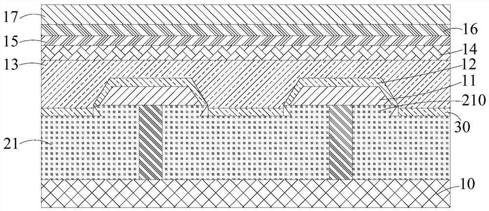
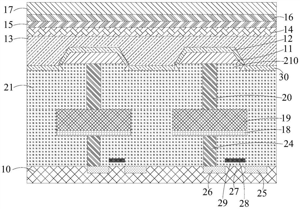
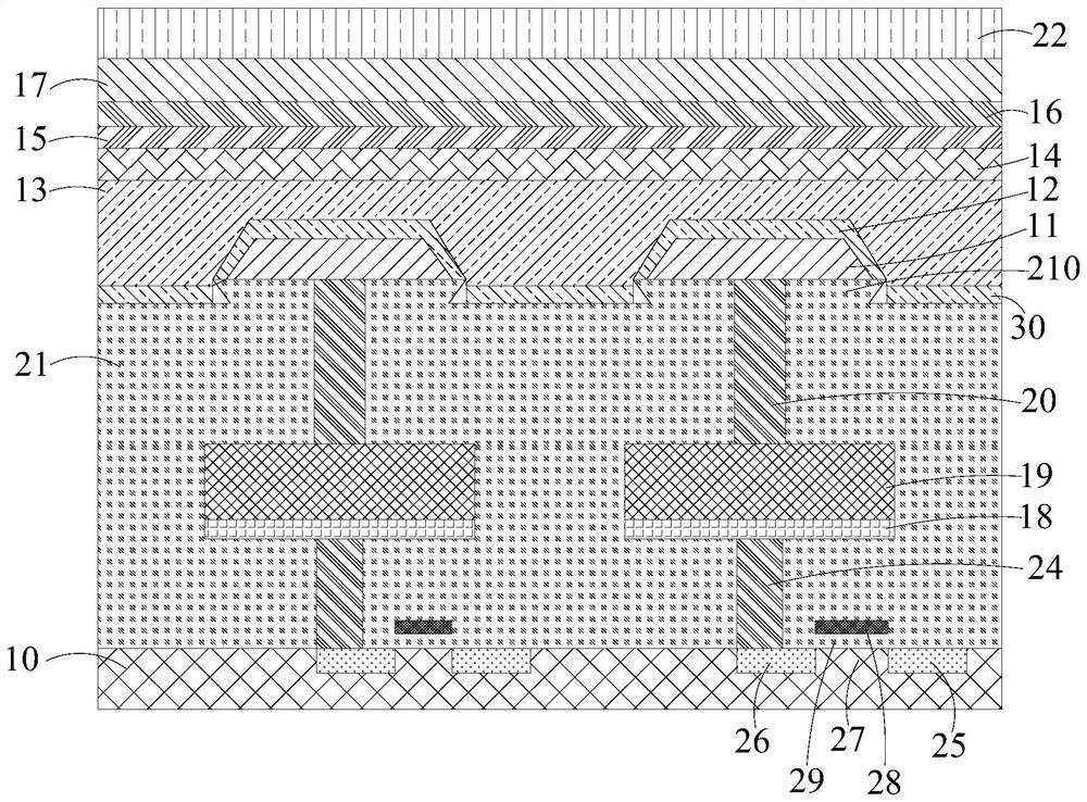
[0053] An example embodiment will now be described more fully with reference to the accompanying drawings. However, exemplary embodiments can be implemented in various forms and should not be construed as limited to the embodiments set forth herein; rather, these embodiments are provided so that this disclosure will be thorough and complete, and the concept of example embodiments will fully convey the A technician in the art. The same reference numerals in the figure indicate the same or similar configuration, and thus the detailed description thereof will be omitted.

[0054]Although the relative reference of the icon is used in this specification, one component of the icon is described for the relative relationship of the icon for another component, but these terms are used in this specification only for convenience, such as according to the drawings. The direction of the example described. It will be appreciated that if the device of the icon is flipped to reverse it, the compo...


PUM


Abstract

The invention relates to an organic electroluminescence structure, a manufacturing method thereof and a display device. The organic electroluminescent structure comprises: a substrate; a passivation protection layer which is formed on one side of the substrate, wherein a plurality of internally tangent parts arranged at intervals are formed on the side, away from the substrate, of the passivation protection layer, each internally tangent part is provided with a first face facing the substrate and a second face away from the substrate, and the orthographic projection of the first face on the substrate is located in the orthographic projection of the second face on the substrate, and a non-zero distance is formed between the edge of the first surface and the edge of the second surface; an anode layer which comprises a plurality of anodes which are arranged at intervals, and each anode is correspondingly formed on the second surface; an organic light-emitting functional layer which is provided with a hole injection layer, wherein the hole injection layer comprises a plurality of hole injection blocks which are arranged at intervals, and each hole injection block is correspondingly formed on one anode; and a cathode layer which is formed on one side, deviating from the anode layer, of the organic light-emitting functional layer. According to the scheme, the crosstalk problem can be improved.

Description

Technical field [0001] The present application relates to the field of display, in particular, to an organic electroluminescence structure and a production method thereof, a display device. Background technique [0002] OLED (Organic Light-Emitting Diodes, organic light emitting diode) display technology as a new type of display technology has been widely used in smart watches, mobile phones, tablet computers, monitors, and other fields. OLED display as silicon using silicon as an active backplane driver, having a high pixel density, highly integrated, small, easy to carry, seismic performance, low power consumption and other outstanding features, the study of the technology currently displayed hotspot One. [0003] However, the existing silicon-based OLED prone to problems of crosstalk (Crosstalk) occurs between the different sub-pixels, one important reason is that since the hole injection layer (HIL) in direct contact with the whole layer of the anode layer is disposed togethe...

Claims


Application Information

Patent Timeline
IPC IPC(8): H01L51/50H01L51/56H01L27/32
CPCH10K59/12H10K50/17H10K50/84H10K71/00H10K59/123H10K59/126H10K50/813H10K50/81H10K50/82H10K50/844H10K2102/351
Inventor 刘李卢鹏程杨盛际张逵
Owner BOE TECH GRP CO LTD
Why Eureka
Try Eureka