Method for forming a semiconductor structure

A semiconductor and gas technology, applied in the field of semiconductor structure formation, can solve problems such as via hole expansion and short circuit, and achieve the effect of avoiding short circuit

Pending Publication Date: 2021-07-09
SEMICON MFG INT (SHANGHAI) CORP +1
View PDF0 Cites 0 Cited by
  • Summary
  • Abstract
  • Description
  • Claims
  • Application Information

AI Technical Summary

Problems solved by technology

However, when the existing self-alignment process forms the through hole, the problem of the expansion of the through hole will occur, which will cause the metal line adjacent to the connected lower layer metal line after the conductive plug is filled in the through hole. A bridge occurs between them, resulting in a short circuit

Method used


Image

  • Method for forming a semiconductor structure
  • Method for forming a semiconductor structure
  • Method for forming a semiconductor structure

Examples


Embodiment Construction

[0022] It can be seen from the background art that the existing self-aligned via process has the problem of via hole enlargement.

[0023] Figure 1 to Figure 4 It is a structural schematic diagram of a method for forming a semiconductor structure in an embodiment of the prior art.

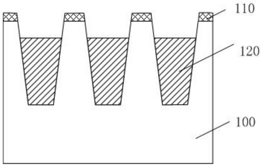
[0024] refer to figure 1 , providing a semiconductor structure, the semiconductor structure comprising a first interlayer dielectric layer 100, a cover layer 110 located on the surface of the first interlayer dielectric layer 100, and a cover layer located between the first interlayer dielectric layer 100 and the cover layer The first metal layer 120 in 110 , the top of the first metal layer 120 is lower than the top surface of the first interlayer dielectric layer 100 .

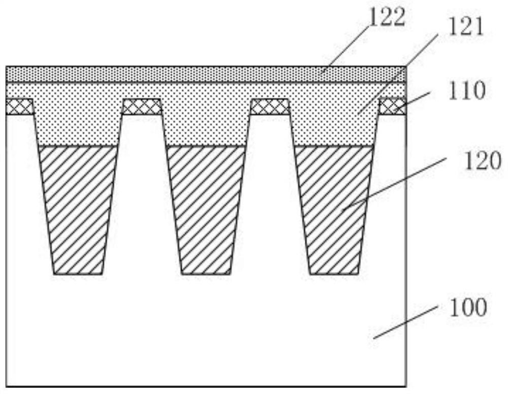
[0025] refer to figure 2 , sequentially forming a barrier layer 121 and an etching stop layer 122 on the surface of the first metal layer 120 , and the barrier layer 121 and the etching stop layer 122 also cover the surface ...


PUM


Abstract

A method for forming a semiconductor structure comprises the following steps: providing a semiconductor substrate, and forming a first dielectric layer on the semiconductor substrate; forming a plurality of discrete first metal layers in the first dielectric layer, wherein the tops of the first metal layers are higher than the top surface of the first dielectric layer; forming a second dielectric layer on the first dielectric layer between the adjacent first metal layers; performing oxidation treatment on the first metal layer to form a metal oxide layer; forming a third dielectric layer on the surfaces of the second dielectric layer and the metal oxide layer; and etching the third dielectric layer until the metal oxide layer is exposed to form a through hole. According to the forming method, the through hole can be formed in a self-alignment mode, the limitation of the bottom size of the through hole is enlarged, and the short circuit problem is avoided.

Description

technical field [0001] The invention relates to the technical field of semiconductor manufacturing, in particular to a method for forming a semiconductor structure. Background technique [0002] As the production of integrated circuits develops towards ultra-large-scale integrated circuits (ULSI), the internal circuit density is increasing, and the number of components contained is increasing, so that the surface of the wafer cannot provide enough area to make the required interconnection lines. (Interconnect). In order to meet the increased demand for interconnection lines after the shrinkage of components, the design of multilayer metal interconnection lines with more than two layers realized by using through holes has become a method that must be adopted in VLSI technology. [0003] However, with the continuous reduction of semiconductor process nodes, the metal interconnection lines in semiconductor devices are becoming denser and the critical dimensions (CD) of interco...

Claims


Application Information

Patent Timeline
IPC IPC(8): H01L21/768
CPCH01L21/76816H01L21/76897H01L2221/101
Inventor 张海洋刘盼盼
Owner SEMICON MFG INT (SHANGHAI) CORP
Why Eureka
Try Eureka