
Directional heteroepitaxy method and silicon-based germanium tin alloy material

A heterogeneous epitaxy and crystal orientation technology, applied in sustainable manufacturing/processing, electrical components, climate sustainability, etc., can solve problems such as difficulties, achieve crystal quality advantages, and shorten the effect of complex growth cycles

Pending Publication Date: 2021-07-13
INST OF SEMICONDUCTORS - CHINESE ACAD OF SCI
View PDF6 Cites 4 Cited by
  • Summary
  • Abstract
  • Description
  • Claims
  • Application Information

AI Technical Summary

Problems solved by technology

[0003] With the potential application prospects of GeSn alloy materials in optoelectronics and microelectronics, it is very meaningful to study and prepare GeSn alloy materials, but there are still many difficulties in how to grow GeSn alloys with high Sn content and high quality

Method used


Image

  • Directional heteroepitaxy method and silicon-based germanium tin alloy material
  • Directional heteroepitaxy method and silicon-based germanium tin alloy material
  • Directional heteroepitaxy method and silicon-based germanium tin alloy material

Examples


Embodiment Construction

[0029] In order to make the object, technical solution and advantages of the present invention clearer, the present invention will be further described in detail below in conjunction with specific embodiments and with reference to the accompanying drawings.

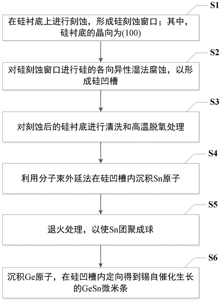
[0030] figure 1 A flow chart of a method for directional heteroepitaxy according to an embodiment of the present disclosure is schematically shown.

[0031] Such as figure 1 As shown, the present disclosure provides a method for directional heteroepitaxy, the method comprising:

[0032] In step S1, etching is performed on the silicon substrate to form a silicon etching window; wherein, the crystal orientation of the silicon substrate is (100).

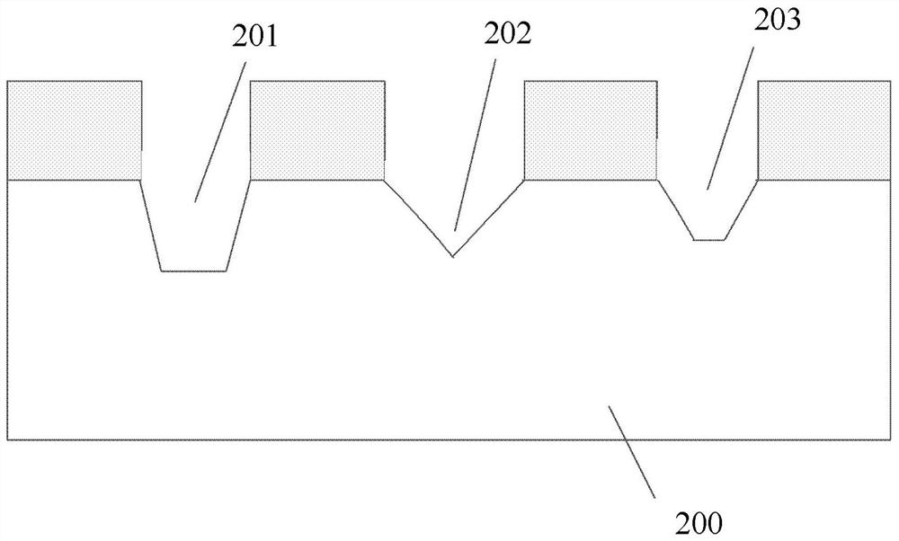
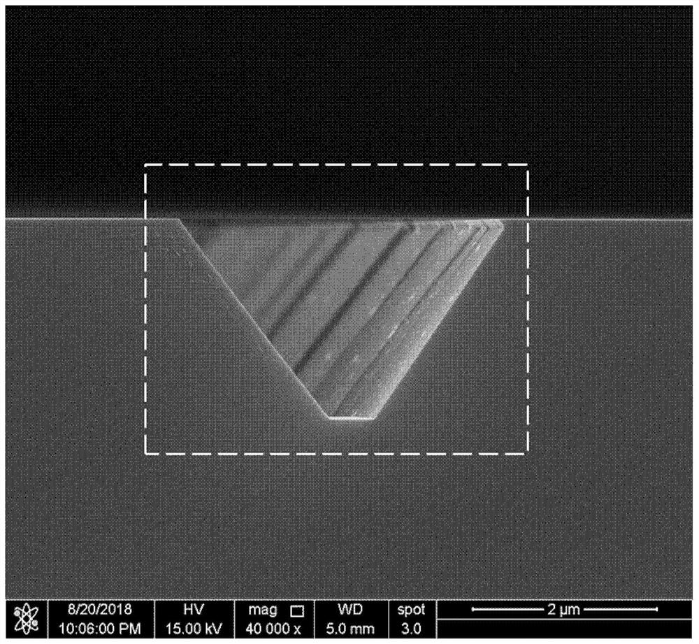
[0033] In step S2, anisotropic wet etching of silicon is performed on the silicon etching window to form silicon grooves.

[0034] In step S3, the etched silicon substrate is cleaned and deoxidized at high temperature.

[0035] In step S4, Sn atoms are deposited in the silicon...


PUM

PropertyMeasurementUnit
thicknessaaaaaaaaaa

Abstract

The invention provides a directional heteroepitaxy method and a silicon-based germanium tin alloy material. The method comprises the following steps of S1, etching on a silicon substrate to form a silicon etching window, wherein the crystal orientation of the silicon substrate is (100); S2, performing anisotropic wet etching of silicon on the silicon etching window to form a silicon groove; S3, carrying out cleaning and high-temperature deoxidation treatment on the etched silicon substrate; S4, depositing Sn atoms in the silicon groove by using a molecular beam epitaxy method; S5, annealing toagglomerate Sn into a ball; and S6, depositing the Ge atoms, and obtaining a GeSn micron strip with tin growing in an autocatalysis mode in the silicon groove in an oriented mode. The invention provides a macrolattice mismatch material system epitaxy method which shortens the growth period of the traditional buffer layer epitaxy and is expected to develop the large-scale device preparation and application.

Description

technical field [0001] The disclosure relates to the technical field of preparation of semiconductor materials, in particular to a directional heterogeneous epitaxy method and a silicon-based germanium-tin alloy material. Background technique [0002] As the most widely used semiconductor material in microelectronic devices, silicon has advantages that other materials cannot replace. However, silicon is an indirect bandgap semiconductor with poor optical performance, so silicon integrated circuits are generally limited to processing electrical signals and cannot process optical signals. Therefore, the development of optoelectronic circuit technology compatible with silicon-based technology, so that the application of silicon-based manufacturing technology to expand from the field of microelectronics to the field of optoelectronics, has become a subject of continuous exploration. Ge and Sn, which are both group IV elements, are expected to become light sources in Si-based op...

Claims


Application Information

Patent Timeline
Patent Type & Authority Applications(China)
IPC IPC(8): H01L31/18H01L21/02H01L31/028
CPCH01L31/1812H01L21/02381H01L21/0243H01L21/02535H01L21/02433H01L21/02631H01L31/028Y02P70/50
Inventor 赵越李传波成步文
Owner INST OF SEMICONDUCTORS - CHINESE ACAD OF SCI
Learn More