Gallium nitride power device gate driving circuit
A technology for gate drive circuits and power devices, applied in electrical components, electronic switches, pulse technology, etc., can solve the problem that level shift circuits do not have anti-interference ability, so as to improve the working ability of floating ground negative pressure, avoid cost, simple structure
- Summary
- Abstract
- Description
- Claims
- Application Information
AI Technical Summary
Problems solved by technology
Method used
Image

Examples
Embodiment Construction
[0046] In order to make the purpose, technical solutions and advantages of the embodiments of the present application clearer, the following will further describe the embodiments of the present application in detail in conjunction with the accompanying drawings.
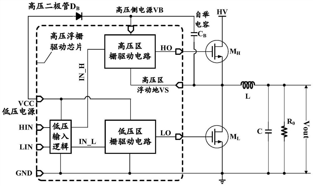
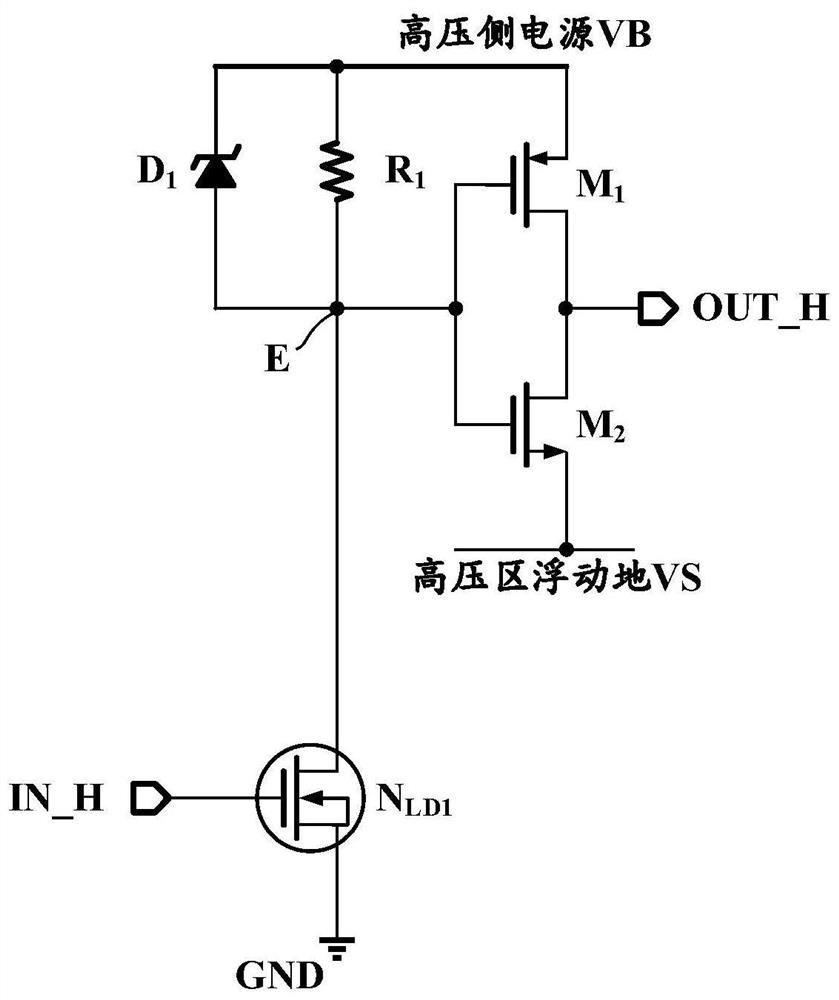
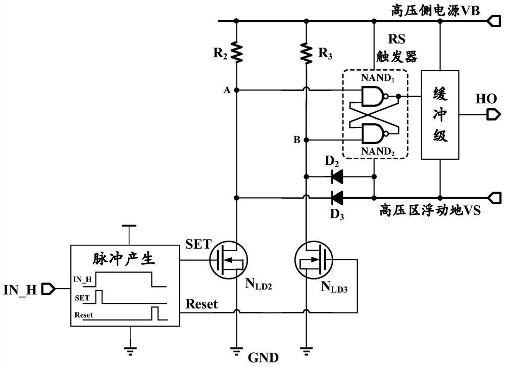
[0047] Please refer to Figure 8 , which shows a structural flowchart of a GaN power device gate drive circuit provided by an embodiment of the present application. The GaN power device gate drive circuit may include: a narrow pulse generation circuit 810 , a high-voltage level shift circuit 820 , a dynamic asymmetric state generation circuit 830 , a common-mode shielding logic 840 , an RS flip-flop 850 and a buffer stage 860 .
[0048] Such as Figure 8 As shown, the input end of the narrow pulse generating circuit 810 is used as the input end IN_H of the GaN power device gate drive circuit, and the first output end SET of the narrow pulse generating circuit 810 is connected to the first input end of the high volta...
PUM
 Abstract
Description
Claims
Application Information
 - Generate Ideas
- Intellectual Property
- Life Sciences
- Materials
- Tech Scout
- Unparalleled Data Quality
- Higher Quality Content
- 60% Fewer Hallucinations
Browse by: Latest US Patents, China's latest patents, Technical Efficacy Thesaurus, Application Domain, Technology Topic, Popular Technical Reports.
© 2025 PatSnap. All rights reserved.Legal|Privacy policy|Modern Slavery Act Transparency Statement|Sitemap|About US| Contact US: help@patsnap.com