A clamping device for semiconductor welding inspection

A welding detection and clamping device technology, applied in workpiece clamping devices, semiconductor devices, semiconductor/solid-state device manufacturing, etc., can solve problems such as failure of electronic products, affecting packaging reliability, etc. Easy-to-use effects

Active Publication Date: 2022-06-21
徐州盛科半导体科技有限公司
View PDF4 Cites 0 Cited by
  • Summary
  • Abstract
  • Description
  • Claims
  • Application Information

AI Technical Summary

Problems solved by technology

Solder joint defects (such as missing solder joints, cracks, virtual soldering, etc.) will seriously affect the reliability of the package, and even make electronic products fail

Method used


Image

  • A clamping device for semiconductor welding inspection
  • A clamping device for semiconductor welding inspection
  • A clamping device for semiconductor welding inspection

Examples


Embodiment 1

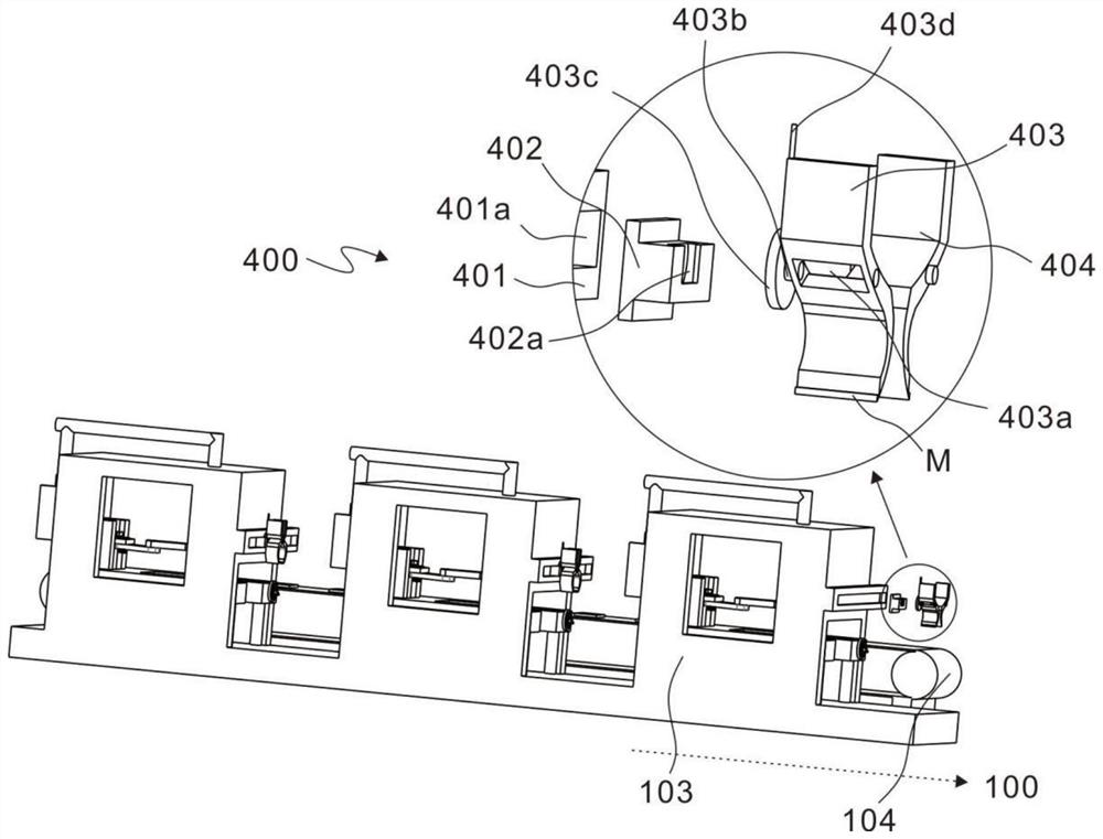
[0027] refer to figure 1 , 2 , which is the first embodiment of the present invention. This embodiment provides a semiconductor welding detection and clamping device, which includes a processing unit 100 and a clamping unit 400 .

[0028] The processing unit 100 includes an operation room 103 and a conveying belt 104. A plurality of operation rooms 103 are arranged in parallel, the conveying belt 104 is arranged on one side of the operation room 103, and the clamping unit 400 is installed on each operation room 103; in the operation room 103 The semiconductor chips are welded or inspected, and then sent to the conveyor belt 104 by the clamping unit 400. All the operation rooms 103 are arranged side by side on one side of the conveyor belt 104 to form an industrial line, which has fast processing efficiency and convenient transportation.

[0029] Further, the clamping unit 400 includes a sliding rail 401, a second sliding block 402, a first clamping member 403 and a second cla...

Embodiment 2

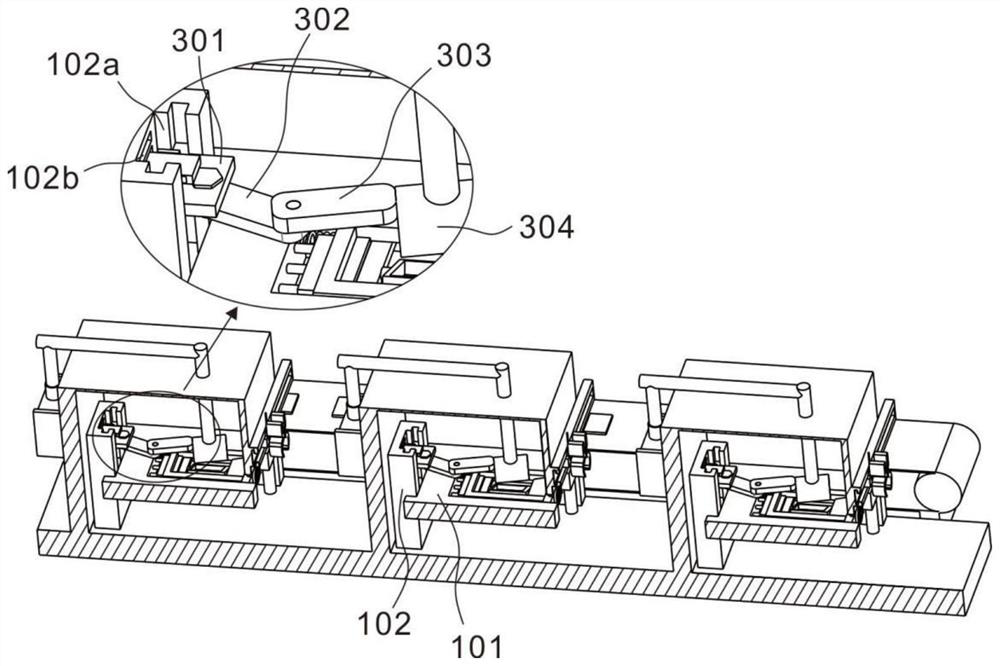
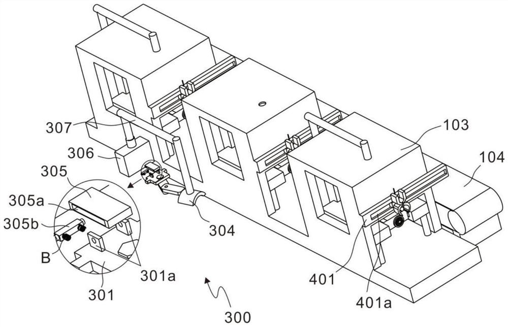
[0035] refer to Figures 2 to 5 , is the second embodiment of the present invention, which is based on the previous embodiment and further includes a dust removal unit 300, which is movably arranged on the adjustment table 102 and faces the platform 101 at the bottom for absorbing the smoke and dust generated by welding and discharged from the operating room 103 .

[0036] The dust removal unit 300 includes a moving plate 301, a turning plate 302, a hinge plate 303 and a dust collector 304. Specifically, the dust removal unit 300 is located above the platform 101 and is connected to the adjusting table 102. The moving plate 301 is movably arranged on the adjusting table 102, and the turning plate 302 One end is bolted to the moving plate 301 , the other end is hinged to the hinge plate 303 , and the other end of the hinge plate 303 is connected to the dust collector 304 .

[0037] Further, a T-shaped groove 102a is vertically disposed on the adjustment table 102, and the T-sh...


PUM


Abstract

The invention discloses a clamping device for semiconductor welding detection, which includes a processing unit, the processing unit includes an operating room and a plurality of conveying belts. The operating rooms are arranged in parallel, and the conveying belt is arranged in one of the operating rooms. side; and a clamping unit, the clamping unit includes a slide rail, a second slider, a first clip and a second clip, the first clip and the second clip are staggered and hingedly arranged, and the first clip The two sliders are arranged in the slide rail, and the first clip and the second clip are connected to the operating room and can be erected on the second slider; the present invention can fixedly install the semiconductor chip, and it is convenient to It is easy to take out or install, and can be rotated at 360 degrees, which is convenient for welding, and the soldered chip does not need to be held by hand, it can be directly clamped out with a clamping piece, and then transported on the conveyor belt, integrated structure, production and transportation more convenient.

Description

technical field [0001] The invention relates to the technical field of semiconductor chip welding, in particular to a semiconductor welding detection and clamping device. Background technique [0002] The development trend of integrated circuit (IC) product miniaturization has put forward higher requirements for chip integration size and packaging reliability. At present, the IC industry widely uses wire bonding technology and flip-chip technology to solve the interconnection problem between multi-layer chips to meet the packaging requirements of electronic products. Regardless of whether wire bonding technology or flip-chip technology is used, multiple solder joints need to be formed on the chip, and then the solder joints are used to complete the interconnection. Solder joint defects (such as missing solder joints, cracks, virtual soldering, etc.) can seriously affect package reliability and even make electronic products fail. SUMMARY OF THE INVENTION [0003] The purp...

Claims


Application Information

Patent Timeline
Patent Type & Authority Patents(China)
IPC IPC(8): H01L21/687H01L21/67H01L21/677B23K37/00B23K37/047B25B11/00
CPCH01L21/687H01L21/67173H01L21/67706B25B11/00B23K37/00B23K37/047B23K2101/40
Inventor 吴龙军廖广兰
Owner 徐州盛科半导体科技有限公司
Why Eureka
Try Eureka