Preparation method of display module and display module

A display module and optical technology, applied in the direction of instruments, electrical components, electric solid devices, etc., can solve the problems of poor flatness and uniformity, loss of light effect, etc., and achieve high controllability, convenient formation, and good adaptability

Active Publication Date: 2021-07-16
广州市鸿利显示电子有限公司
View PDF11 Cites 1 Cited by
  • Summary
  • Abstract
  • Description
  • Claims
  • Application Information

AI Technical Summary

Problems solved by technology

[0004] In order to overcome the technical problems of loss of light efficiency, poor flatness and uniformity existing in the existing preparation method, the embodiment of the present invention provides a method for preparing a display module and a display module

Method used


Image

  • Preparation method of display module and display module
  • Preparation method of display module and display module
  • Preparation method of display module and display module

Examples


Embodiment 1

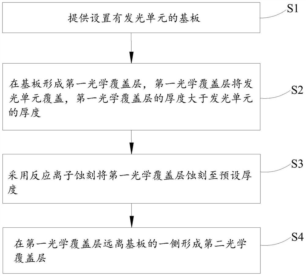
[0061] Please refer to figure 1 This embodiment provides a method of displaying a display module, a preparation method of a display module is used to prepare a display module, which includes the following steps:

[0062] S1 provides a substrate provided with a light-emitting unit;

[0063] S2, the first optical cover layer is formed in the substrate, and the first optical cover layer covers the light-emitting unit, the thickness of the first optical cover layer is larger than the thickness of the light emitting unit;

[0064] S3, the first optical cover layer is etched to a preset thickness using a reaction ion etching;

[0065] S4, the second optical cover layer is formed on one side of the first optical cover layer away from the substrate.

[0066] Among them, the preset thickness refers to the design thickness of the first optical cover layer according to the actual production design, in other words, in the thickness of the first optical cover layer in the finished product. The...

Embodiment 2

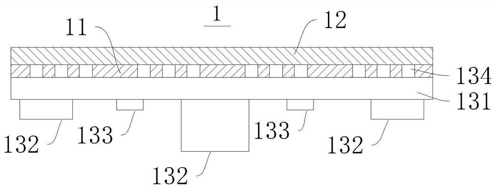
[0116] Please refer to Figure 17 This embodiment provides a display module 3, and the display module 3 is prepared by the preparation method provided in Example 1.

[0117] The display module 3 includes a substrate 331, an electronic component 332, an IC chip 333, an LED chip 334, a first optical cover layer 31, and a second optical cover layer 32.

[0118] The material type of the substrate 331 can generally be BT, FR-4, glass, aluminum plate, FPC, or the like, and is not limited thereto. Optionally, in this embodiment, the material of the substrate 331 is BT.

[0119] The first optical cover layer 31 and the second optical cover layer 32 are formed by optical glue, cured, and optical rubber, silicone, silicone, epoxy resin, and the like, and is not limited thereto. Alternatively, in the present embodiment, optical rubber is an epoxy resin.

[0120] The electronic component 332, the IC chip 333 is attached to the BOTTOM surface of the substrate 331, and the LED chip 334 is mixed ...

Embodiment 3

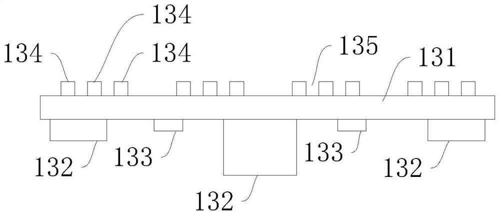
[0127] Please refer to Figure 18 with Figure 19 This embodiment provides a display module 4, and the display module 4 is prepared by the preparation method provided in Example 1. Different from the display module 3 in Example 2, only one LED chip 434 is provided on the substrate 431 of each display module 4, and the first optical cover layer 41 is formed on the substrate 431, and the first optical cover layer is formed. The 41 side of the retained substrate 431 is etched to the side surface of the LED chip 434 away from the substrate 431 from the LED chip 434. The first optical cover layer 41 surrounds the LED chip 434. The second optical cover layer 42 is formed on one side away from the substrate 431 in both the first optical cover layer 41 and the LED chip 434.

[0128] The advantageous effects of the technical solutions provided by the embodiments of the present invention include:

[0129] 1. During the preparation of the display module, before covering the second rubber layer...


PUM

PropertyMeasurementUnit
thicknessaaaaaaaaaa

Abstract

The invention belongs to the field of display components and relates to a preparation method of a display module and a display module.The preparation method comprises the steps that: a substrate provided with a light-emitting unit is provided; a first optical covering layer is formed on the substrate, the first optical covering layer covers the light-emitting unit, and the thickness of the first optical covering layer is larger than that of the light-emitting unit; the first optical covering layer is etched to a preset thickness by adopting reactive ion etching; and a second optical covering layer is formed on one side, far away from the substrate, of the first optical covering layer. The flatness and uniformity of an etched surface can be guaranteed, and the product quality and the light emitting effect are improved. The display module is prepared through the preparation method, and the light emitting effect of the display module is good.

Description

[Technical field] [0001] The present invention relates to the field of displaying components, and in particular, to a preparation method of a display module and a display module. 【Background technique】 [0002] Currently, during the preparation of the display module, it is often necessary to remove excess rubber layers. Conventional cleaning mode / removal method includes two physical etching and chemical etching, after physical etching, it is easy to affect the appearance of the product and the loss of light efficiency, and chemical etching can easily lead to anisotropy, so that The overall surface flatness and uniformity have become very poor, which directly affects the quality and use effects. [0003] In view of this, this application will be put forward. [Summary] [0004] In order to overcome the technical problem of the loss, flatness, and uniformity of the existing preparation method, the embodiment of the present invention provides a method of displaying a display modul...

Claims


Application Information

Patent Timeline
Patent Type & Authority Applications(China)
IPC IPC(8): H01L25/075H01L33/54H01L33/58G09F9/33
CPCH01L25/0753H01L33/54H01L33/58G09F9/33H01L2933/0058H01L2933/005
Inventor 常德良陈永铭桑建颜春明
Owner 广州市鸿利显示电子有限公司
Why Eureka
Try Eureka