Microlens array, pixel island 3D display device and preparation method thereof

A technology of microlens array and lens array, applied in the field of 3D display, can solve the problems of light field 3D image crosstalk and moiré change

Pending Publication Date: 2021-07-23
BOE TECH GRP CO LTD
View PDF0 Cites 0 Cited by
  • Summary
  • Abstract
  • Description
  • Claims
  • Application Information

AI Technical Summary

Problems solved by technology

[0005] The purpose of this application is to provide a microlens array, a pixel island 3D display device and a preparation method thereof, so as to solve the problem that in the prior art, the light rays at a certain angle can only meet the condition of collimating the focal plane to emit light, which causes the human eye As the viewing angle changes, the 3D image of the light field seen has technical problems such as large crosstalk and moiré changes

Method used


Image

  • Microlens array, pixel island 3D display device and preparation method thereof
  • Microlens array, pixel island 3D display device and preparation method thereof
  • Microlens array, pixel island 3D display device and preparation method thereof

Examples


Embodiment 1

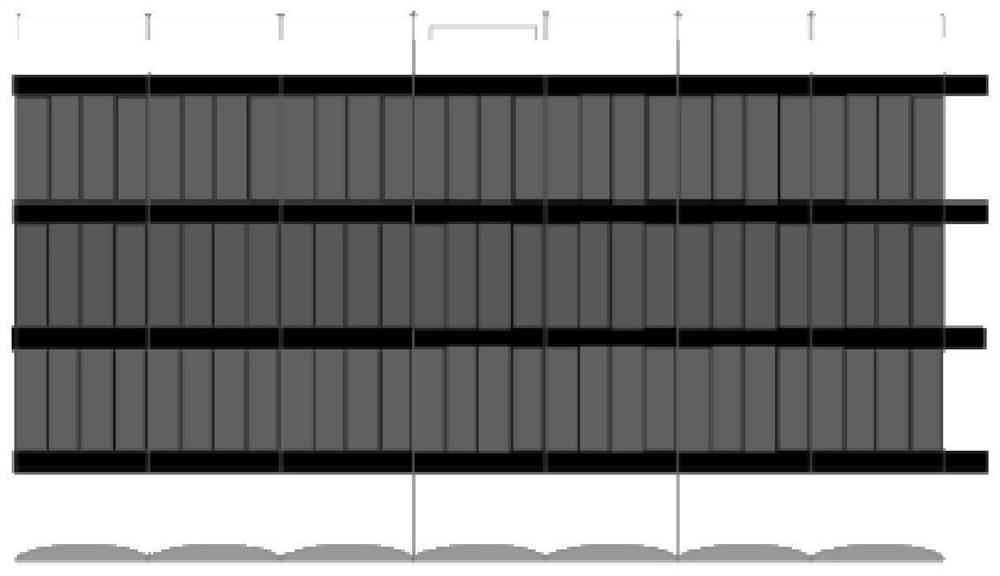
[0055] In order to solve the above technical problems, such as Figure 7-Figure 9 As shown, the present application provides a microlens 5 array, including: a first driving electrode 1, a liquid crystal film 2, a second driving electrode 3 and an organic medium layer 4 that are sequentially stacked along the light emitting direction of the display screen 6, preferably , the first driving electrode 1 and the second driving electrode 3 are arranged in a continuous structure, wherein the first driving electrode 1 and the second driving electrode 3 cover all sub-pixels 7; in a specific embodiment, the The outside of the lens 5 array structure is also wrapped with a flat layer 11; the organic medium layer 4 is provided with a lens 5 array structure, wherein the lens shape shown in this embodiment is not limited to the spherical shape shown in the figure, but also It can also be applied to cylindrical lenses, and the shape of the lens is not limited in this embodiment; under the act...

Embodiment 2

[0070] Compared with the array of microlenses 5 provided in Embodiment 1, the array of microlenses 5 proposed in this embodiment has the following differences: Figure 10 and Figure 11 As shown, one of the first driving electrode 1 and the second driving electrode 3 is set as a subdivision electrode, and the other is set as a continuous structure. In a specific embodiment, as Figure 10 As shown, the first driving electrode 1 is configured as a continuous structure, and the second driving electrode 3 is configured as a subdivided electrode. Preferably, the subdivided electrodes correspond to a plurality of sub-pixels 7 one by one; specifically, the scheme of the first embodiment is adopted After many experiments, the voltage difference required for each sub-pixel 7 is determined, and then the second driving electrode 3 shown in Embodiment 1 is refined, so that the second driving electrode 3 corresponding to each sub-pixel 7 Apply the required voltage difference; when it is n...

Embodiment 3

[0077] Compared with the array of microlenses 5 provided in Embodiment 1, the array of microlenses 5 proposed in this embodiment has the following differences: Figure 13 As shown, the first driving electrode 1 and the second driving electrode 3 are both configured as subdivision electrodes.

[0078]According to an embodiment of the present invention, the subdivision electrodes correspond to a plurality of sub-pixels 7 one-to-one. Of course, each sub-electrode in the subdivision electrodes corresponds to a plurality of sub-pixels 7. Of course, a one-to-many arrangement The corresponding resolution is lower than the resolution corresponding to the one-to-many setting method. In actual use, it is preferable to adopt a one-to-one correspondence between multiple sub-electrodes in the subdivision electrodes and the sub-pixels 7. On the one hand, the resolution can be guaranteed, and on the other hand, On the one hand, precise control of each sub-pixel 7 can also be realized. To sum...


PUM


Abstract

The invention relates to the technical field of 3D display, in particular to a microlens array, a pixel island 3D display device and a preparation method thereof. The microlens array comprises a first driving electrode, a liquid crystal film, a second driving electrode and an organic dielectric layer which are sequentially arranged in a stacked mode in the light emitting direction of a display screen, and a lens array structure is arranged on the organic dielectric layer; and under the action of a voltage difference formed between the first driving electrode and the second driving electrode, the refractive index of the liquid crystal film is controlled to change in the direction of reducing the placement height of the edge sub-pixel, so that the focus of the edge sub-pixel is adjusted to a corresponding focal arc surface. In conclusion, by adopting the design of the invention, the light rays emitted by the sub-pixels at any angle can meet the focal plane collimation light emitting condition, so that the optimal-quality main lobe viewing angle region of the light field 3D can be received no matter where human eyes are located, and the ultra-low crosstalk, the moire and the ultra-large visual space are realized.

Description

technical field [0001] The invention relates to the technical field of 3D display, in particular to a microlens array, a pixel island 3D display device and a preparation method thereof. Background technique [0002] Among the five major perception pathways of human beings, vision accounts for 70% to 80% of the information sources, and about 50% of the brain's ability is used to process visual information. From daily behavior to complex operations, it is highly dependent on our visual perception; however, the existing image acquisition and display loses multi-dimensional visual information, which forces us to observe the three-dimensional world only through two-dimensional "windows"; light Field display is a method for us to obtain multi-dimensional visual information. It can simulate the way the human eye perceives light and focuses, and dynamically focuses on the area where the human eye gazes, presenting a more natural sense. [0003] Pixel island light field 3D display c...

Claims


Application Information

Patent Timeline
Patent Type & Authority Applications(China)
IPC IPC(8): G02B30/28G02F1/13G02F1/1343
CPCG02F1/13G02F1/134309G02B30/28
Inventor 孙艳六梁蓬霞石戈刘玉杰
Owner BOE TECH GRP CO LTD
Why Eureka
Try Eureka