Method for manufacturing substrate for electronic device, method for manufacturing electronic device, substrate for electronic device, and electronic device

A technology of electronic devices and manufacturing methods, which is applied in the field of improving the light extraction structure of optical devices, and can solve problems such as extraction, failure, and inability to extract emitted light

Active Publication Date: 2011-12-21
ASAHI GLASS CO LTD
View PDF7 Cites 0 Cited by
  • Summary
  • Abstract
  • Description
  • Claims
  • Application Information

AI Technical Summary

Problems solved by technology

At this time, since the angle of incidence on the glass substrate does not change, it is repeatedly reflected in the organic layer and the light-transmitting electrode layer, and cannot be extracted from the glass substrate to the outside.
It is estimated that about 60% of the emitted light cannot be extracted due to this mode (organic layer-translucent electrode layer propagation mode)
The same situation occurs at the interface between the substrate and the atmosphere, whereby about 20% of the emitted light propagates inside the glass, and the light cannot be extracted (substrate propagation mode)
Therefore, the current situation is that the amount of light that can be extracted to the outside of the organic LED element is less than 20% of the emitted light

Method used


Image

  • Method for manufacturing substrate for electronic device, method for manufacturing electronic device, substrate for electronic device, and electronic device
  • Method for manufacturing substrate for electronic device, method for manufacturing electronic device, substrate for electronic device, and electronic device
  • Method for manufacturing substrate for electronic device, method for manufacturing electronic device, substrate for electronic device, and electronic device

Examples


no. 1 approach

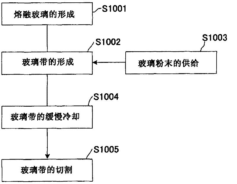
[0047] The manufacturing method of the electronic device substrate of the present invention, such as process flow figure 1 As shown, it is characterized in that it includes the following steps: a step of heating and melting glass raw materials or glass to produce molten glass (step S1001); continuously supplying molten glass to a bath of a molten metal bath (molten metal tank) containing molten metal surface to form a continuous glass ribbon forming process (step S1002); supply glass powder with a desired composition on the continuous glass ribbon, and form a scattering layer by melting the glass powder (step S1003); The process of slowly cooling the continuous glass ribbon with a scattering layer (step S1004); the process of cutting the slowly cooled continuous glass ribbon with a scattering layer to obtain a glass substrate with a scattering layer (step S1005).

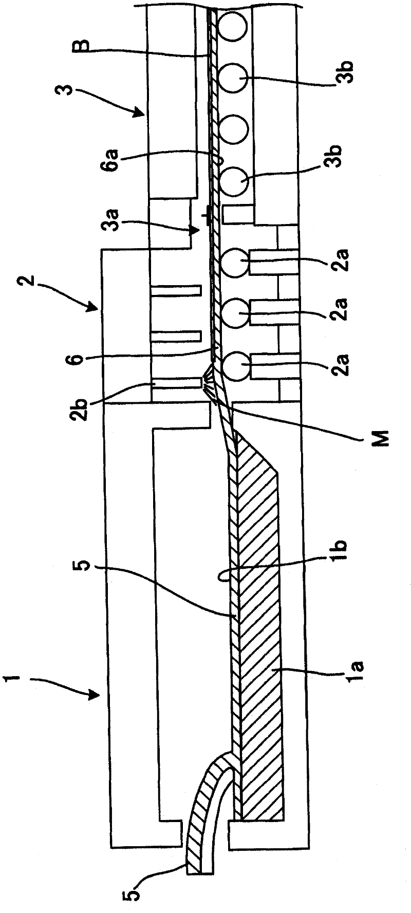
[0048] figure 2 It is a schematic cross-sectional view showing a part of the manufacturing equipment used in th...

no. 2 approach

[0088] Next, a second embodiment of the present invention will be described.

[0089] In addition, in the first embodiment, the glass layer as the scattering layer B is formed by spraying the suspension from the nozzle 2b at the entrance of the transport chamber 2 while forming the glass ribbon 6 as the substrate. In the second embodiment, as Figure 5 As shown in the enlarged view of the main part of the manufacturing device, it is characterized in that the scattering layer B is formed by directly spraying the glass powder onto the substrate (glass ribbon 6) by electrostatic powder spraying. This implementation uses roughly as figure 2 Shown is the same device as the device of Embodiment 1, but an electrostatic powder spraying device is provided on the back side of the glass ribbon (refer to figure 2 ), a scattering layer forming device is installed at the entrance of the slow cooling chamber 3, and nip portions (not shown) are provided at predetermined intervals instead ...


PUM

PropertyMeasurementUnit
Horizontal lengthaaaaaaaaaa
Surface roughnessaaaaaaaaaa

Abstract

A method for producing a substrate for an electronic device, that can improve light extraction efficiency, can easily produces and has high liability is provided. The method includes: a step of heat-melting a glass raw material or a glass to produce a molten glass; a forming step of continuously feeding the molten glass to a bath surface of a molten metal bathtub accommodating a molten metal to form a continuous glass ribbon 6; a step of feeding a glass powder M having a desired composition on the continuous glass ribbon 6 and melting or sintering the glass powder M to form a scattering layer; a step of gradually cooling the scattering layer-attached continuous glass ribbon; and a step of cutting the scattering layer-attached continuous glass ribbon gradually cooled to obtain a scattering layer-attached glass substrate.

Description

technical field [0001] The invention relates to a method for manufacturing a substrate for an electronic device, a method for manufacturing an electronic device, a substrate for an electronic device, and an electronic device, in particular to an improvement technology for light extraction structures of optical devices such as organic LEDs (organic light-emitting diodes). Background technique [0002] The organic LED element sandwiches the organic layer between the electrodes, applies a voltage between the electrodes, injects holes and electrons to recombine in the organic layer, and extracts the light generated during the process of the light-emitting molecules from the excited state to the ground state. The components are, therefore, used in displays, backlights, and lighting applications. [0003] The organic layer has a refractive index of about 1.8 to about 2.1 at 430 nm. On the other hand, for example, when ITO (Indium Tin Oxide: Indium Tin Oxide) is used as the light-...

Claims


Application Information

Patent Timeline
IPC IPC(8): C03C17/04H01L51/50H05B33/02
CPCC03C17/008C03C3/21H05B33/02C03C2217/77C03C8/08C03C17/04C03C2217/48Y10T428/24926Y02E10/549Y02P70/50H10K77/10H10K50/854
Inventor 中村伸宏山田兼士松本修治
Owner ASAHI GLASS CO LTD
Why Eureka
Try Eureka