Flexible electronic paper electronic display equipment and manufacturing method thereof
An electronic display and manufacturing method technology, applied in nonlinear optics, optics, instruments, etc., can solve the problems of limited bending angle, high cost and high process of electronic paper, and achieve the effects of low cost, simple molding and weight reduction
- Summary
- Abstract
- Description
- Claims
- Application Information
AI Technical Summary
Problems solved by technology
Method used
Image
Examples
Embodiment 1
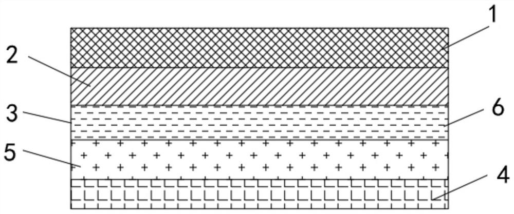
[0027] Such as figure 1 As shown, a flexible electronic paper electronic display device includes a flexible base layer 1, the bottom of the flexible base layer 1 is bonded with an LED chip 2, the bottom of the LED chip 2 is provided with a circuit layer 3, and the circuit layer 3 includes a conductive layer 4 and an insulating layer 5 , the top of the conductive layer 4 is provided with an insulating layer 5, the top surface of the insulating layer 5 is provided with an ink layer 6, the top surface of the ink layer 6 is electrically connected to the LED chip 2, and the flexible base layer 1 is a PDLC substrate. In the design of the flexible display , Injection considers avoiding short circuit of crossing lines. In order to make the flexible display screen as transparent as possible when passing through, the amount of printed lines should be made small under the inlay to ensure the conduction of the lines. In order to avoid crossing lines, an ink layer 6 is used. , the insulati...
Embodiment 2
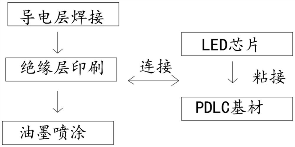
[0029] Such as figure 1 and figure 2 As shown, a method for manufacturing a flexible electronic paper electronic display device includes the following steps:
[0030] Sp1: The circuit layer 3 is welded into the conductive layer 4 with a circuit with a diameter of 50±5μm, and baked in a drying oven at 100° for 20 minutes;
[0031] Sp2: The circuit layer 3 is provided with insulating bumps on the top surface of the connection node of the conductive layer 4 to form an insulating layer 5, and put it in a drying oven at 110° for 30 minutes;
[0032] Sp3: heat the conductive ink into a slurry by heating it in a high-temperature heating box;
[0033] Sp4: The surface of the insulating layer 5 is printed and sprayed with conductive ink to form the ink conductive layer 4, put it in a drying oven and bake at 110° for 30 minutes;
[0034] Sp5: Paste the LED chip 2 on the surface of the PDLC substrate by using the crystal-bonding process, place it in a drying oven at 120° for 40 minut...
PUM
| Property | Measurement | Unit |
|---|---|---|
| diameter | aaaaa | aaaaa |
| thickness | aaaaa | aaaaa |
| thickness | aaaaa | aaaaa |
Abstract
Description
Claims
Application Information

