How to make pcb

A production method and technology of crimping holes, which are applied in the fields of printed circuit manufacturing, printed circuits, printed circuit components, etc., can solve the problems of increasing the thickness of finished PCBs, unfavorable insertion and installation of components, and uneven surface of PCBs, etc., to achieve improved Improve the quality, improve the flatness, and reduce the difficulty of PCB production

Active Publication Date: 2022-06-21
DONGGUAN SHENGYI ELECTRONICS
View PDF6 Cites 0 Cited by
  • Summary
  • Abstract
  • Description
  • Claims
  • Application Information

AI Technical Summary

Problems solved by technology

[0004] 1. The low flow prepreg remaining outside the crimp hole area will increase the thickness of the finished PCB;
[0005] 2. High and low steps are formed between the crimping holes and through holes, resulting in uneven surface of the PCB, which is not conducive to the subsequent insertion and installation of components on the PCB, seriously affecting the user experience

Method used


Image

  • How to make pcb
  • How to make pcb
  • How to make pcb

Examples


Embodiment Construction

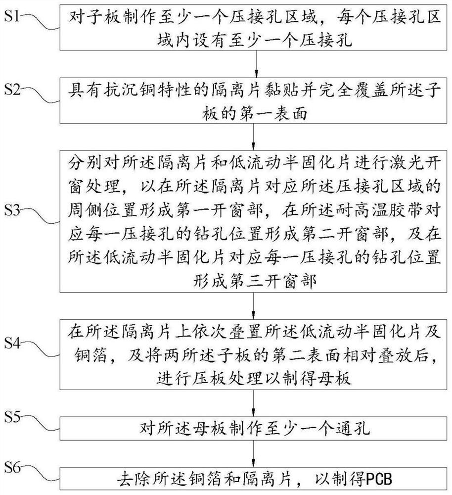
[0049] In order to describe the technical content, structural features, achieved objects and effects of the present invention in detail, the following detailed description is given in conjunction with the embodiments and the accompanying drawings.

[0050] see Figure 1-Figure 13 As shown, the PCB 100 of the present embodiment is manufactured by a manufacturing method of a PCB, and the manufacturing method of the PCB includes the following steps:

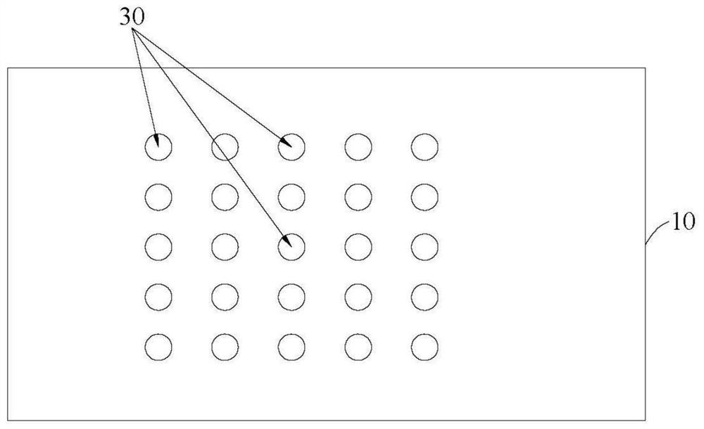
[0051] S1 , at least one crimping hole area 20 is formed on the sub-board 10 , and each crimping hole area 20 is provided with at least one crimping hole 30 .

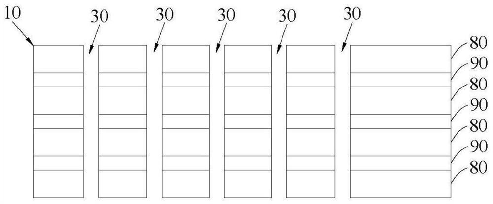
[0052] It can be understood that the drawings involved in this embodiment are all illustrated with one of the crimping hole regions 20 of the PCB 100 , and the number of the crimping hole regions 20 of the PCB 100 may be one, two, three or four, etc. . The crimping hole area 20 is provided with a plurality of image 3 The shown crimping holes 30 penetrating the first surf...


PUM


Abstract

The invention discloses a PCB manufacturing method and the PCB. The manufacturing method includes: making a crimping hole area on a sub-board; pasting a spacer with anti-sinking copper characteristics and completely covering the first surface of the sub-board; Laser window processing to form a first window opening on the peripheral side of the crimping hole area, and a second window opening at the drilling position of each crimping hole; stack low flow prepreg and copper in sequence on the separator Foil, and after laminating the low-flow prepreg between the second surfaces of the two sub-boards, press the plate to make the mother board; make through holes on the mother board; remove the copper foil and the spacer to make the PCB; the present invention can A PCB with a flat surface and a small thickness can be obtained, which can effectively avoid the formation of high and low steps on the surface of the crimping holes and through holes of the PCB due to the low-flow prepreg remaining outside the crimping hole area, and effectively reduce the subsequent components on the PCB. The difficulty of plugging and installation effectively improves the user experience.

Description

technical field [0001] The invention relates to the technical field of PCB (Printed Circuit Board, printed circuit board), and in particular, to a manufacturing method of the PCB. Background technique [0002] In the prior art, the asymmetric design of the double-sided crimping holes of the PCB is mainly made by the double-sided crimping process of the N+N method. The hole is protected to avoid damage to the crimping hole due to the potion biting the crimping hole in the wet process process such as potion biting involved in the production of the via hole. [0003] However, when the sub-board is fabricated in the prior art, it is necessary to etch away the outer copper layer of the sub-board except the crimping hole area, only keep the outer layer copper on the sub-board crimping hole area, and press the low-flow prepreg correspondingly. The position of the contact hole area is opened, and then the low-flow prepreg and the whole copper foil board are pressed on the sub-board...

Claims


Application Information

Patent Timeline
Patent Type & Authority Patents(China)
IPC IPC(8): H05K3/00H05K3/42H05K1/02
CPCH05K3/00H05K3/42H05K3/0047H05K1/02
Inventor 刘潭武王小平陈长平纪成光
Owner DONGGUAN SHENGYI ELECTRONICS
Why Eureka
Try Eureka