Plane wave to spherical wave phased array chip based on graphene metasurface

A metasurface, graphene technology, applied in electrical components, antennas, etc., can solve problems such as excessive loss and narrow bandwidth, and achieve the effect of large phase modulation range and easy processing

Pending Publication Date: 2021-08-20
HUAQIAO UNIVERSITY
View PDF0 Cites 0 Cited by
  • Summary
  • Abstract
  • Description
  • Claims
  • Application Information

AI Technical Summary

Problems solved by technology

[0004] The purpose of the present invention is to overcome the deficiencies of the prior art, and propose a phased array chip from plane wave to spherical wave based on graphene metasurface, which is used to solve the technical problems of excessive loss and narrow bandwidth in the prior art

Method used


Image

  • Plane wave to spherical wave phased array chip based on graphene metasurface
  • Plane wave to spherical wave phased array chip based on graphene metasurface
  • Plane wave to spherical wave phased array chip based on graphene metasurface

Examples


Embodiment Construction

[0026] In order to make the object, technical solution and advantages of the present invention clearer, the embodiments of the present invention will be further described in detail below in conjunction with the accompanying drawings.

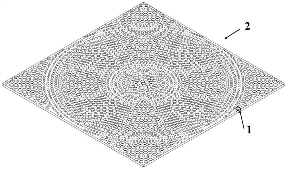
[0027] see figure 1 As shown, it is a schematic diagram of the three-dimensional structure of the graphene metasurface-based plane wave to spherical wave phased array chip of the present embodiment, and the graphene metasurface-based plane wave to spherical wave phased array chip includes M×M graphene Metasurface unit 1, M=50 in this specific embodiment, the mutual seamless arrangement between each graphene metasurface unit 1 constitutes a reflective metasurface phased array 2 of cuboid structure, this reflective metasurface phased array The surface size of the array 2 is 50 microns x 50 microns.

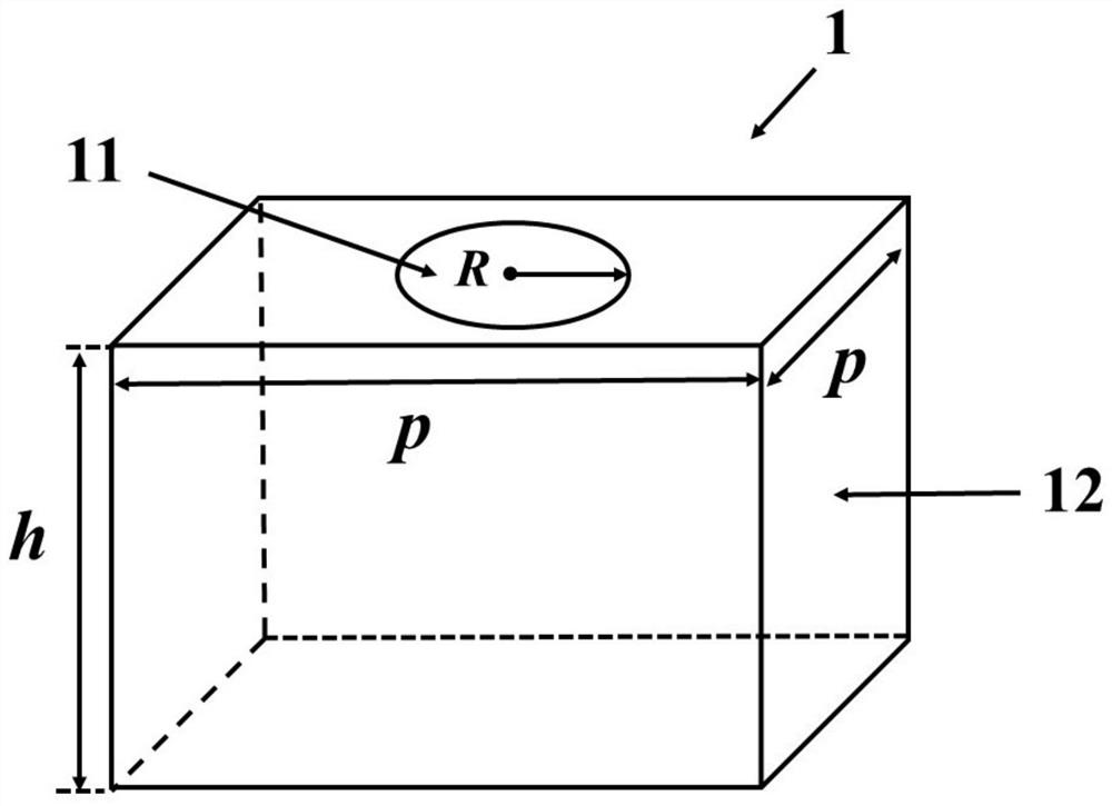
[0028] see figure 2 Shown is a schematic diagram of a three-dimensional structure of a single graphene metasurface unit 1, which includes a graphe...


PUM

PropertyMeasurementUnit
radiusaaaaaaaaaa
lengthaaaaaaaaaa
thicknessaaaaaaaaaa

Abstract

The invention provides a plane wave to spherical wave phased array chip based on a graphene metasurface. The plane wave to spherical wave phased array chip comprises a reflective metasurface phased array. The reflective metasurface phased array comprises M * M graphene metasurface units which are arranged periodically; each graphene metasurface unit comprises a graphene patch of which the upper surface is a circular structure and a lower dielectric substrate; and the graphene patch with the circular structure and the geometric center of the dielectric substrate below are on the same straight line. By utilizing the characteristic that each graphene metasurface unit can enable an electric field of an incident wave to generate 0-360-degree all-phase regulation and control, the function of converting a plane wave into a spherical wave is realized in a frequency range of 50 THz to 60 THz, and the advantages of a wide frequency band, planarization and a single-layer structure are possessed.

Description

technical field [0001] The invention relates to the field of wireless communication, in particular to a phased array chip from plane wave to spherical wave based on graphene metasurface. Background technique [0002] In recent years, with the rapid development of wireless communication technology, people have higher and higher requirements on the performance and size of devices. Electromagnetic metasurface is a two-dimensional planar array composed of periodic or non-periodic subwavelength unit structures, which has extraordinary physical properties that natural materials do not have. Electromagnetic metasurface is a kind of electromagnetic material with two-dimensional structure, which is relatively light and thin, has the characteristics of small volume and simple structure, and can flexibly control the amplitude, phase and polarization state of electromagnetic waves (Xiangang, L.Principles of Electromagnetic Waves in Metasurface[J].ScienceChina,2015,58(9):594201), is wid...

Claims


Application Information

Patent Timeline
Patent Type & Authority Applications(China)
IPC IPC(8): H01Q15/14H01Q3/30
CPCH01Q3/30H01Q15/14
Inventor 马焕喜邱伟彬
Owner HUAQIAO UNIVERSITY
Why Eureka
Try Eureka