
Sample preparation method

A sample preparation and sample technology, applied in electrical components, electrical solid devices, circuits, etc., can solve problems such as affecting electrical stability and the difficulty of samples to meet electrical testing.

Active Publication Date: 2021-08-27
YANGTZE MEMORY TECH CO LTD
View PDF7 Cites 0 Cited by
  • Summary
  • Abstract
  • Description
  • Claims
  • Application Information

AI Technical Summary

Problems solved by technology

[0003] However, because the internal structure of the 3D memory is too tightly distributed in space, the SSRM test results of the sample will be affected by the nearby conductive structures during the SSRM scanning process, which will affect its electrical stability, making it difficult for the sample to meet the requirements of the electrical test. Require

Method used


Image

  • Sample preparation method
  • Sample preparation method
  • Sample preparation method

Examples


Embodiment Construction

[0029] Exemplary embodiments disclosed in the present application will be described in more detail below with reference to the accompanying drawings. Although exemplary embodiments of the present application are shown in the drawings, it should be understood that the present application may be embodied in various forms and should not be limited to the specific embodiments set forth herein. Rather, these embodiments are provided for a more thorough understanding of the present application and for fully conveying the scope disclosed in the present application to those skilled in the art.

[0030] In the following description, numerous specific details are given in order to provide a more thorough understanding of the present application. It will be apparent, however, to one skilled in the art that the present application may be practiced without one or more of these details. In other examples, in order to avoid confusion with the present application, some technical features kno...


PUM


Abstract

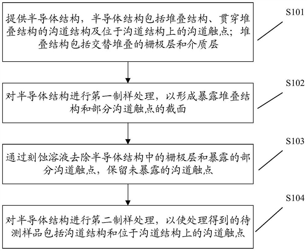
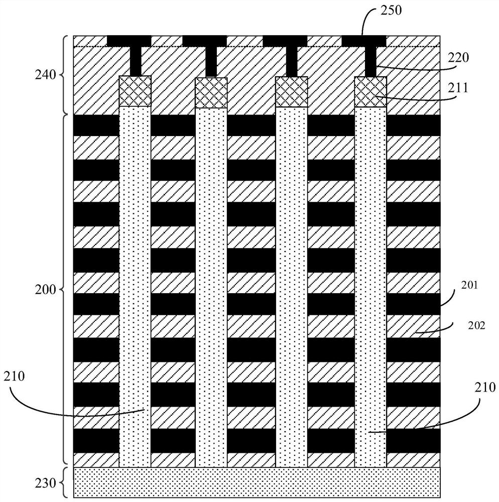
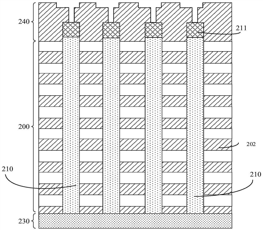
The invention discloses a sample preparation method, and the method comprises the steps: providing a semiconductor structure which comprises a stacking structure, a channel structure penetrating through the stacking structure, and a channel contact located on the channel structure, wherein the stacked structure comprises gate layers and dielectric layers which are alternately stacked; performing first sample preparation processing on the semiconductor structure to form a cross section exposing the stack structure and a part of the channel contact; removing the gate layer in the semiconductor structure and the exposed part of the channel contact through an etching solution, and reserving the unexposed channel contact; and carrying out second sample preparation treatment on the semiconductor structure, so that a to-be-tested sample obtained through treatment comprises the channel structure and the channel contact located on the channel structure.

Description

technical field [0001] The present application relates to the field of semiconductor technology, in particular to a sample preparation method. Background technique [0002] In 3D memory, the doping distribution of the channel plug and the common source of the array plays an important role in the electrical properties of 3D NAND products. Direct data cannot be obtained by conventional electrical tests. Generally, only scanning expansion resistors can be used. Microscopy (Scanning Spreading Resistance Microscopy, SSRM) physical characterization method is used for testing, and a conductive diamond probe is used to scan the surface of the sample to obtain a two-dimensional distribution map of the spreading resistance, thereby reflecting the carrier doping distribution. [0003] However, because the internal structure of the 3D memory is too tightly distributed in space, the SSRM test results of the sample will be affected by the nearby conductive structures during the SSRM scann...

Claims


Application Information

Patent Timeline
Patent Type & Authority Applications(China)
IPC IPC(8): H01L27/1157H01L27/11582H01L23/544H10B43/35H10B43/27
CPCH01L22/32H10B43/35H10B43/27
Inventor 陈茜卫晓阳锁志勇
Owner YANGTZE MEMORY TECH CO LTD
Learn More