PCB defect image recognition method based on multi-model fusion convolutional neural network

A convolutional neural network and image recognition technology, applied in the field of PCB defect image recognition based on multi-model fusion convolutional neural network, can solve the problems of high labor intensity and achieve the effect of good classification and recognition performance

Active Publication Date: 2021-09-03
SHANGHAI UNIV
View PDF7 Cites 0 Cited by
  • Summary
  • Abstract
  • Description
  • Claims
  • Application Information

AI Technical Summary

Problems solved by technology

[0004] The object of the present invention is to aim at the deficiencies in the prior art, provide a kind of PCB defect image recognition method based on multi-model fusion convolutional neural network, act on many kinds of PCB defect image overcomes the problems of traditional manual PCB defect detection, such as high labor intensity and low work efficiency, can reduce the cost of manual visual inspection on the post-sequence verification and repair system station, improve production efficiency, and realize automatic and intelligent identification of PCB defect categories

Method used


Image

  • PCB defect image recognition method based on multi-model fusion convolutional neural network
  • PCB defect image recognition method based on multi-model fusion convolutional neural network
  • PCB defect image recognition method based on multi-model fusion convolutional neural network

Examples


Embodiment 1

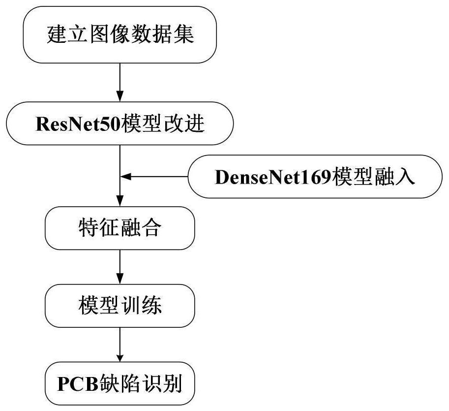
[0039] See body 1~ Figure 6 , a PCB defect image recognition method based on multi-model fusion convolutional neural network, the operation steps are as follows:

[0040] (1) Establish an image data set: obtain multiple types of PCB defect images, establish a PCB image data set, and classify according to each defect type;

[0041] (2) ResNet50 model improvement;

[0042] Improve the shortcomings of the existing deep convolutional neural network model, and establish a convolutional neural network framework suitable for PCB defect image recognition;

[0043] (3) Feature Fusion:

[0044] In order to further improve the effect of PCB defect classification and recognition, a PCB defect recognition method based on multi-model fusion is proposed; image features extracted based on multiple models are fused, and the output network structure of the fused features is improved;

[0045] (4) Model training to realize PCB defect identification:

[0046] The PCB picture set is divided int...

Embodiment 2

[0049] This embodiment is basically the same as Embodiment 1, and the special features are as follows:

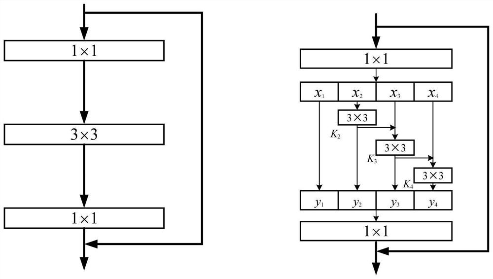
[0050] The step (2) improves the shortcomings of the existing deep convolutional neural network model, and establishes a convolutional neural network framework suitable for PCB defect image recognition. The ResNet50 network structure consists of four large BottleNecks. Each block is composed of 3, 4, 6, and 3 small residual blocks. Each small residual block is composed of 1×1, 3× 3. Three 1×1 convolutional layers are connected in series; in addition, the front end and the last end of the network are respectively composed of a 7×7 convolutional layer, a maxpool layer and an average pooling layer. The optimized and improved ResNet50 model introduces a new type of CNN module called Res2Net, which replaces the residual blocks containing 1×1, 3×3, and 1×1 convolutional layers in the original ResNet50 with more hierarchical residual blocks. Differentiate the connection structure...

Embodiment 3

[0054] see figure 1 , a PCB defect image recognition method based on multi-model fusion convolutional neural network, which includes the following steps:

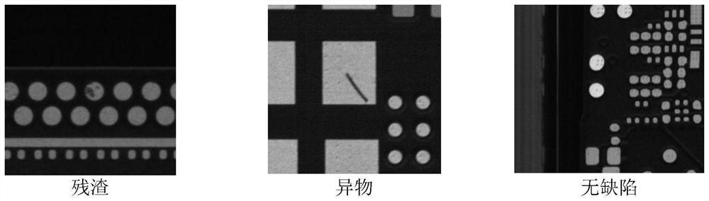
[0055] Obtain multiple types of PCB defect images and non-defect images, use various data enhancement methods to expand the image set and establish a PCB image data set, and classify it according to each defect type. The present invention selects two kinds of defects, residue and foreign matter, and after data enhancement, there are 3900 pieces of each kind of defect in the training set, and 7800 pieces of non-defective PCB images. The test set has a total of 5200 pictures, including 1300 pictures of residue and foreign matter defects, and 2600 pictures without defects. figure 2 There are two kinds of defect pictures of residue and foreign matter and no defect pictures, which are sorted out by experienced staff.

[0056] To improve the shortcomings of the existing deep convolutional neural network model, a ResNet50 convo...


PUM


Abstract

The invention discloses a PCB defect image recognition method based on an improved convolutional neural network. In order to overcome the defects of an existing ResNet50 deep convolutional neural network model, a novel CNN module named Res2Net is introduced, and a residual connection structure and an activation function are changed, so that the multi-layer nonlinear expansion capability of the network is improved. Based on an improved ResNet50 model, a DenseNet169 convolutional neural network is fused, fusion is carried out based on image features extracted by multiple models, a fusion feature output network structure is improved, and a multi-model fused convolutional neural network framework for PCB defect image recognition is established. The method can identify different types of PCB defect images, has the characteristics of high identification accuracy and sensitivity compared with a single model, and can realize automatic and intelligent identification of PCB defect types.

Description

technical field [0001] The invention relates to the field of defect detection, in particular to a PCB defect image recognition method based on a multi-model fusion convolutional neural network. Background technique [0002] As the basic pillar of the development of electronic information industry, printed circuit board (PCB) is widely used in industrial control, communication, medical treatment, aviation and other fields. With the advancement of my country's science and technology and industrial upgrading, PCB defect detection technology has become a vital link in economic production. However, the visual inspection machine based on the automatic optical inspection system has a high false alarm rate in PCB defect detection, resulting in high cost and low work efficiency for subsequent verification and manual visual inspection at the repair system station. Therefore, it is particularly important to use deep learning technology to identify PCB defects. [0003] In recent year...

Claims


Application Information

Patent Timeline
Patent Type & Authority Applications(China)
IPC IPC(8): G06K9/62G06N3/04G06N3/08
CPCG06N3/08G06N3/045G06F18/24G06F18/25G06F18/214
Inventor 张健滔瞿栋汪鹏宇黄允徐海达
Owner SHANGHAI UNIV
Why Eureka
Try Eureka