Spot-size converter and silicon optical integrated chip

An integrated chip and converter technology, applied in the field of optical communication, can solve the problems of large wedge-shaped structure loss, large polarization-dependent loss, and large polarization-dependent loss of mode spot converter.

Active Publication Date: 2021-09-07
INNOLIGHT TECHNOLOGY (SUZHOU) LTD
View PDF8 Cites 1 Cited by
  • Summary
  • Abstract
  • Description
  • Claims
  • Application Information

AI Technical Summary

Problems solved by technology

However, the tip of the wedge-shaped structure is limited by the semiconductor processing technology, so it is difficult to make the size infinitely small, and it is easy to introduce polarization-dependent loss, that is, when the light is gradually changing from a thinner thickness waveguide to a normal thickness waveguide, the horizontally polarized mode (TE mode) light The loss is small, the vertically polarized mode (TM mode) has a large loss of light, and the overall mode spot converter has a large

Method used


Image

  • Spot-size converter and silicon optical integrated chip
  • Spot-size converter and silicon optical integrated chip
  • Spot-size converter and silicon optical integrated chip

Examples


Embodiment 1

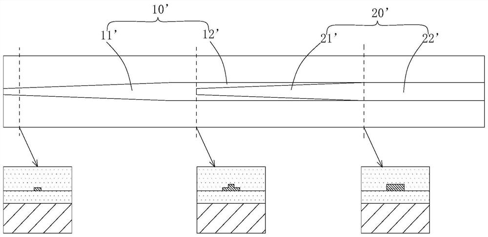
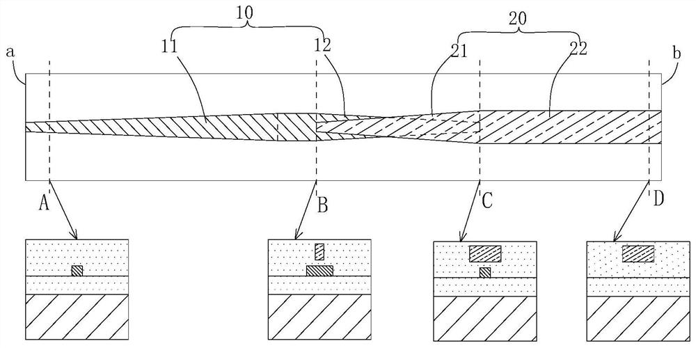
[0036] Such as image 3 and 4, this embodiment provides a mode spot converter, which has a first end face a optically coupled with an external optical fiber and a second end face b optically coupled with an external optical device, the mode spot converter includes a first optical waveguide 10 and a second optical waveguide Two optical waveguides 20 , the thickness of the first optical waveguide 10 is smaller than the thickness of the second optical waveguide 20 . Wherein, the first optical waveguide 10 includes a first wedge-shaped structure 11 and a second wedge-shaped structure 12, the tip of the first wedge-shaped structure 11 is close to the above-mentioned first end face a, and the tip of the second wedge-shaped structure 12 faces to the edge of the first wedge-shaped structure 11. Orientation of the tips facing away from each other. Here, the tip of the first wedge-shaped structure 11 is close to the above-mentioned first end face a, which means that the tip of the fir...

Embodiment 2

[0040] Such as Figure 5 As shown, the difference from Embodiment 1 is that the second optical waveguide 20 of the speckle converter in this embodiment adds an edge coupling structure 23, and one end of the edge coupling structure 23 is connected to the tip of the third wedge-shaped structure 21, and the other One end deviates from the central axis of the second optical waveguide 20 and extends toward the edge of the first optical waveguide 10 to better adiabatically couple the optical modes in the first optical waveguide 10 into the second optical waveguide 20 .

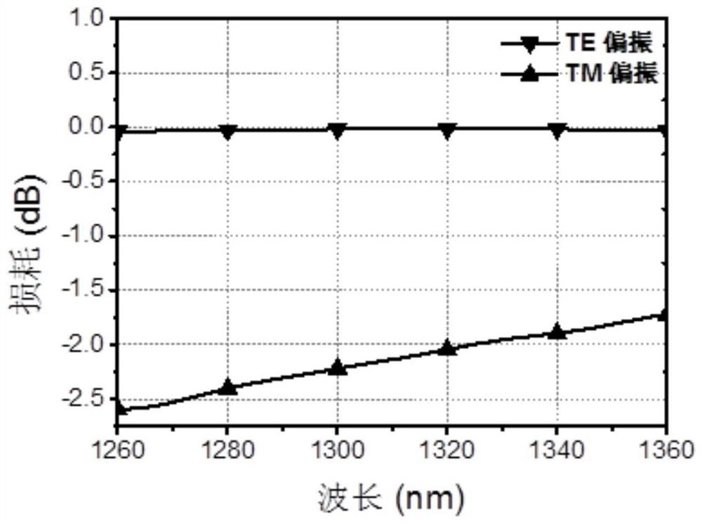
[0041] In the speckle converter of Embodiment 1, in order to reduce the polarization-dependent loss between the first optical waveguide 10 and the second optical waveguide 20 as much as possible, the tip size of the third wedge-shaped structure 21 of the second optical waveguide 20 needs to be made to be as small as possible, but limited by the semiconductor processing technology, the tip of the third wedge-shaped s...

Embodiment 3

[0044] Such as Figure 7 As shown, the difference from Embodiments 1 and 2 is that the first end face a of the speckle converter in this embodiment is provided with a hollowed out portion 40 at the substrate 31 of the lower cladding layer 32 under the first optical waveguide 10 , for example, a hollow portion 40 can be etched on the end face a of the substrate 31 by using a wet etching process, so as to bind the light beams in the upper cladding layer 34, the lower cladding layer 32 and the first optical waveguide 10, and avoid external optical fiber The light coupled to the first optical waveguide 10 enters the substrate 31 and is radiated and lost from the substrate, thereby further improving the coupling efficiency between the external optical fiber and the mode-spot converter.


PUM

PropertyMeasurementUnit
Thicknessaaaaaaaaaa
Thicknessaaaaaaaaaa
Widthaaaaaaaaaa

Abstract

The invention discloses a spot-size converter and a silicon optical integrated chip. The spot-size converter has a first end surface optically coupled with an external optical fiber and a second end surface optically coupled with an external optical device, and the spot-size converter comprises a first optical waveguide and a second optical waveguide, wherein the first optical waveguide comprises a first wedge-shaped structure and a second wedge-shaped structure, and the first wedge-shaped structure and the second wedge-shaped structure face opposite directions; and the second optical waveguide comprises a third wedge-shaped structure, and the tip of the third wedge-shaped structure faces the first wedge-shaped structure and is at least partially overlapped with the second wedge-shaped structure. By designing a special waveguide coupling structure, the mode matching degree of the spot-size converter and the external optical fiber is improved, the polarization dependent loss between the two optical waveguides in the spot-size converter is reduced, and the thermal stability of the optical waveguides in the silicon optical integrated chip is improved, so that the optical transmission loss in the silicon optical integrated chip is reduced.

Description

technical field [0001] The present application relates to the technical field of optical communication, in particular to a speckle converter and a silicon optical integrated chip. Background technique [0002] Silicon photonics chip is the key technology to realize optical interconnection, which can effectively reduce the cost of modules in optical communication. However, at the coupling point between the optical fiber and the silicon photonics chip, the size of a typical single-mode silicon waveguide is 420nm×220nm, while the size of a single-mode fiber is about 9 μm. efficient coupling between them. Currently, common coupling solutions include a vertical coupling method of a grating coupler and a horizontal coupling method of a Spot Size Converter (SSC). The grating coupler makes a grating structure on the silicon waveguide. When the light is incident on the surface of the grating coupler from the optical fiber, it can be effectively coupled with the optical fiber placed...

Claims


Application Information

Patent Timeline
IPC IPC(8): G02B6/14G02B6/122G02B6/12
CPCG02B6/14G02B6/122G02B2006/12152G02B6/12
Inventor 郭德汾李显尧
Owner INNOLIGHT TECHNOLOGY (SUZHOU) LTD
Why Eureka
Try Eureka