Systems and methods for detecting endpoint for through-silicon via reveal applications

a technology of reveal application and through-silicon, which is applied in the field of optical imaging, can solve the problems of tsv nodes protruding too much from the silicon, becoming increasingly difficult to precisely detect the change in emission, and enhancing the pattern matching effect, so as to achieve the effect of precise detection and matching, enhancing the pattern matching, and improving the accuracy of matching

Active Publication Date: 2017-01-10
LAM RES CORP
View PDF13 Cites 0 Cited by
  • Summary
  • Abstract
  • Description
  • Claims
  • Application Information

AI Technical Summary

Benefits of technology

[0016]The advantages of the present invention over the prior art are numerous. One notable benefit and advantage of the invention is that the camera(s) is able to capture the emerging pattern of infinitesimally small dimensions and match the emerging pattern to a reference pattern captured at the same angle as the angle used to capture the emerging pattern, in a more reliable fashion. The exposed area of the structures / features especially in TSV reveal process is very small, to the order of less than 0.1% of the semiconductor wafer surface and the selectivity to the TSV structures liner material is very high that conventional OES techniques for endpoint detection do not work reliably and consistently. As a result, conventional methods used a timed-etch process. The timed-etch process results in a large variation in the exposed features / structures height. The various embodiments disclosed herein use the pattern recognition technology to more reliably identify the structures when they emerge on the surface of the substrate and enable realization of a controlled endpoint to the etch operation.
[0017]Another benefit is the ability to take advantage of the viewports that provide access to the interior of the plasma processing chamber and allows precise detection and matching of the pattern emerging during the active etching operation. In some embodiments, multiple cameras may be used to enhance the pattern matching by allowing the cameras to work in tandem to generate three dimensional view of the emerging pattern. In such embodiments, any skewing of images from one camera may be compensated by the images from another camera. In some embodiments, the image processor may include logic to correct the skew of the received images so that matching may be more precise. In some embodiments, the emerging pattern may be skewed due to the angle at which the cameras capture the pattern appearing on the surface of the semiconductor wafer. In such embodiments, the reference pattern used for matching with the emerging pattern is identified such that the angle at which the reference pattern is captured matches with the angle of capture of the emerging pattern.

Problems solved by technology

However, as the features / structures reduce in size, it is becoming increasingly difficult to precisely detect change in emission, especially when the etch process is to have very high selectivity to exposed film around the features / structures.
Due to the high selectivity defined for the etch process, it is very hard to detect when the endpoint for the TSV reveal is reached using the OES technique, as no new species are emitted into the plasma, potentially leading to over-etching of the silicon.
The over-etching may result in the TSV nodes protruding too much from the silicon bulk with potential damage to the TSV nodes during packaging.
However, for applications, such as the TSV Reveal, the main etch process does not use Bias Power in order to achieve high selectivity to a film layer formed over the features / structures.
As a result, no usable changes in RF parameters can be detected when endpoint is reached.
The fixed time approach, however, has its own drawbacks as the approach is still vulnerable to process variations, such as drift in the etch rate or variation in the incoming wafer film thickness, etc., leading to unnecessary and excess variation in the desired results, such as large variation in the height of the structures / features.
The RF technique and the OES signal changes offer extremely low signal to noise ratio and have proven to be inadequate for precisely determining end point for etching processes, especially for the ones that do not use stop film.

Method used


Image

  • Systems and methods for detecting endpoint for through-silicon via reveal applications
  • Systems and methods for detecting endpoint for through-silicon via reveal applications
  • Systems and methods for detecting endpoint for through-silicon via reveal applications

Examples


Embodiment Construction

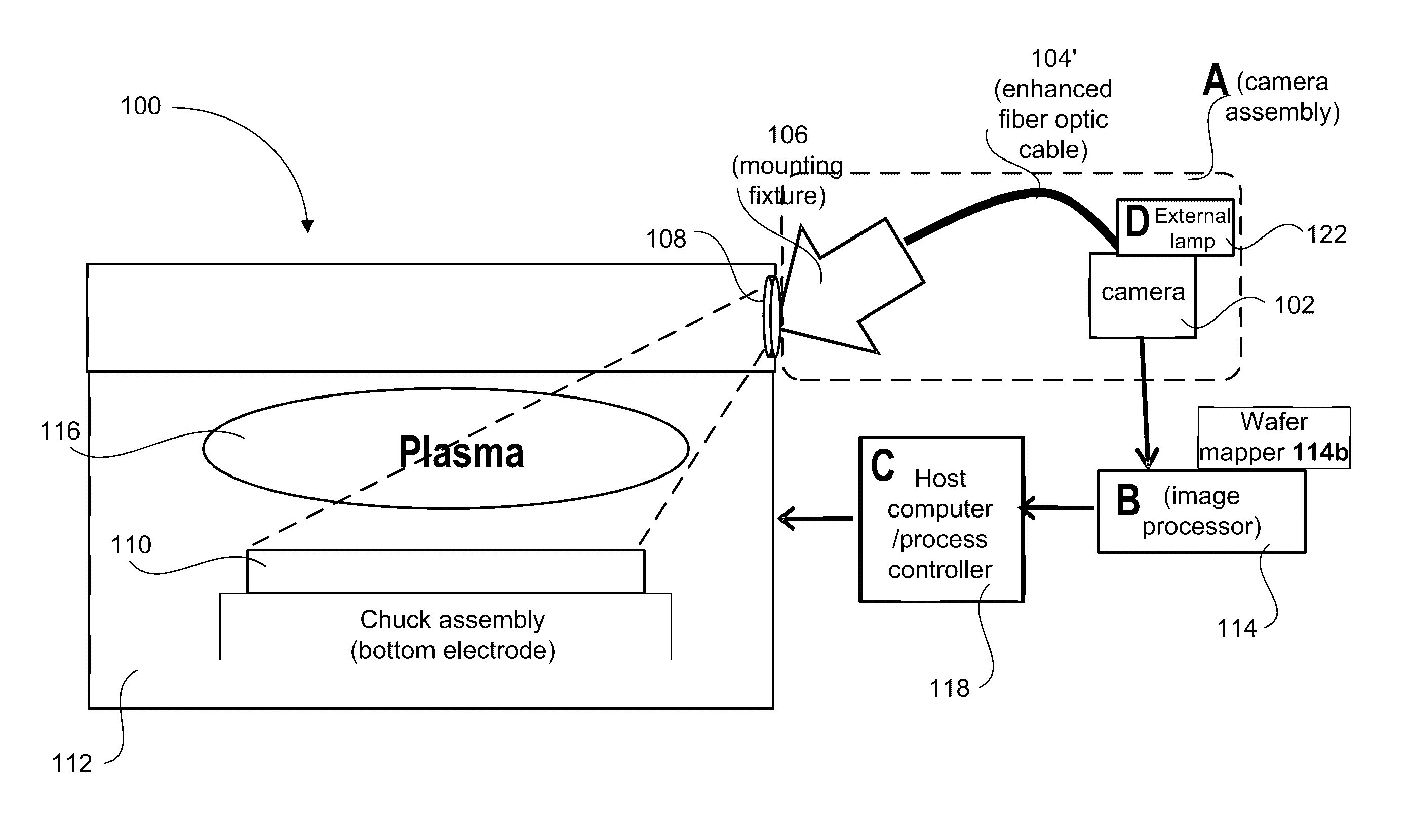
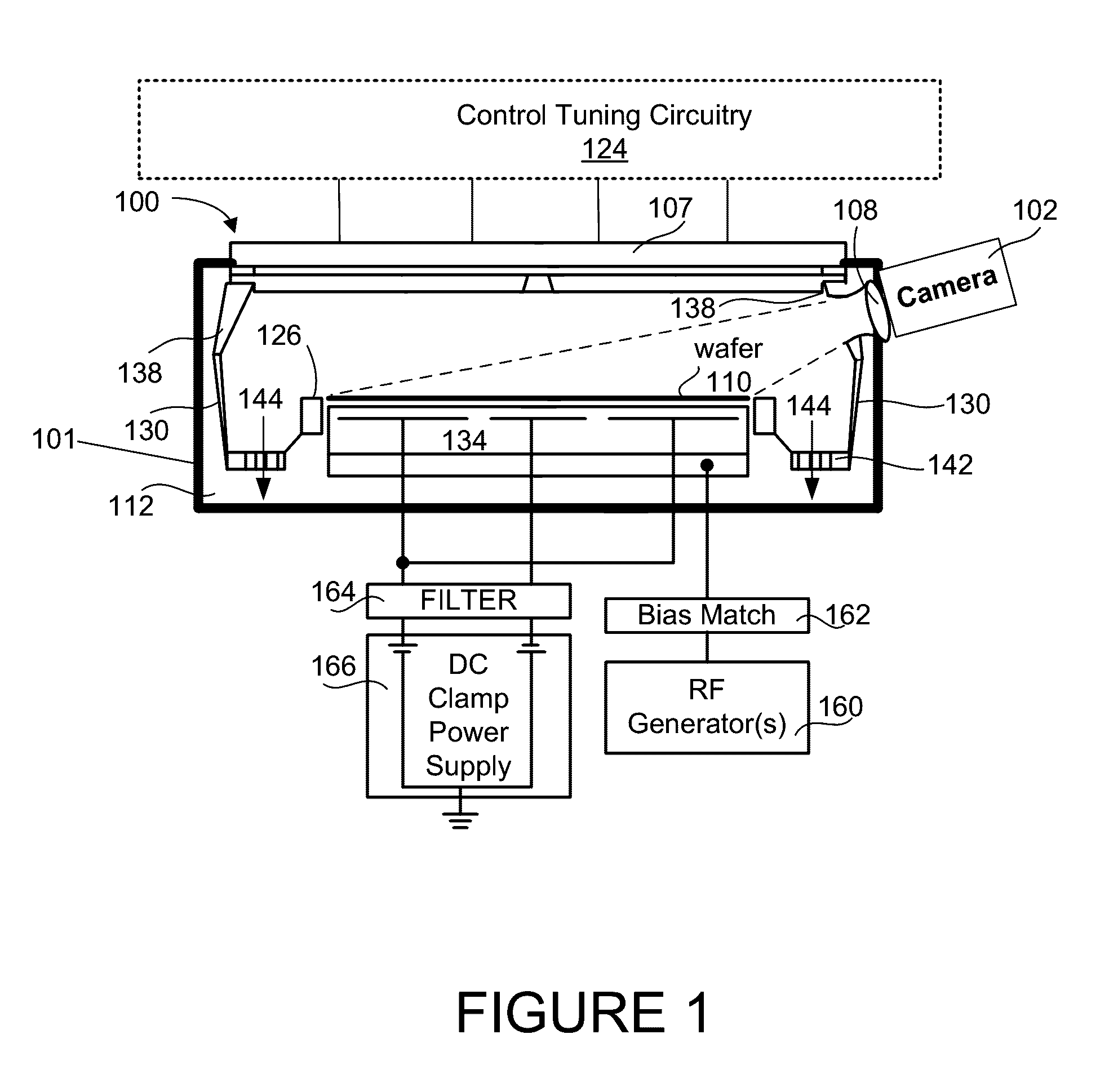
[0028]An invention for determining process end point in plasma etch operations is described. In preferred embodiments, systems for the detection and analysis of images of emerging pattern include providing a camera at a viewport of a plasma processing chamber, capturing a sequence of images of an active surface of a wafer during an etching operation through the viewport using the camera, comparing the emerging pattern of the captured images with a reference pattern and determining when to generate an endpoint call for the etching operation. In the following description, numerous specific details are set forth in order to provide a thorough understanding of the present invention. It will be understood, however, to one skilled in the art, that the present invention may be practiced without some or all of these specific details. In other instances, well known process operations have not been described in detail in order not to unnecessarily obscure the present invention.

[0029]As an ove...


PUM


Abstract

Systems and methods for processing a semiconductor wafer includes a plasma processing chamber. The plasma processing chamber includes an exterior, an interior region with a wafer receiving mechanism and a viewport disposed on a sidewall of the plasma processing chamber providing visual access from the exterior to the wafer received on the wafer receiving mechanism. A camera is mounted to the viewport of the plasma processing chamber on the exterior and coupled to an image processor. The image processor includes pattern recognition logic to match images of emerging pattern captured and transmitted by the camera, to a reference pattern and to generate signal defining an endpoint when a match is detected. A system process controller coupled to the image processor and the plasma processing chamber receives the signal from the image processor and adjusts controls of one or more resources to stop the etching operation.

Description

BACKGROUND OF THE INVENTION[0001]1. Field of the Invention[0002]The present invention relates generally to optical imaging, and more specifically to endpoint detection in semiconductor manufacturing using pattern recognition technology on the images obtained from optic camera.[0003]2. Description of the Related Art[0004]In the fabrication of semiconductor structures such as integrated circuits, memory cells, and the like, features, structures, and components are defined, patterned, and constructed in a series of manufacturing process steps on semiconductor wafers to create multi-layer integrated structures. During the semiconductor manufacturing process, semiconductor wafers are processed through numerous operations in controlled environments to add layers, and to define, pattern, etch, remove, polish, etc., structures, features and layers. The structures and features formed on the semiconductor wafers are closely monitored and analyzed to precisely determine the endpoint of each pr...

Claims


Application Information

Patent Timeline
Patent Type & Authority Patents(United States)
IPC IPC(8): H01L21/66H01L21/768H01L21/3065H01L21/67
CPCH01L22/26H01L21/3065H01L21/67253H01L21/76898H01L22/12
Inventor MILLER, ALAN JEFFREYSEVILLANO, EVELIOLUQUE, JORGEBAILEY, III, ANDREW DXU, QING
Owner LAM RES CORP
Why Eureka
Try Eureka