Resistive layer material, memristor and preparation method thereof

A technology of resistive layer and memristor, which is applied in the direction of electrical components, can solve the problems of changes in multiple resistance states, and it is difficult to simulate the plasticity of human brain synapses.

Active Publication Date: 2021-09-07
LANZHOU UNIVERSITY
View PDF4 Cites 0 Cited by
  • Summary
  • Abstract
  • Description
  • Claims
  • Application Information

AI Technical Summary

Problems solved by technology

[0003] Therefore, the technical problem to be solved by the present invention is to overcome the fact that the memristor in the prior art cannot realize the change of multiple resistance states, and it is difficult to simulate the human brain synapse plasticity defects, thus providing a resistive layer material and memristor

Method used


Image

  • Resistive layer material, memristor and preparation method thereof
  • Resistive layer material, memristor and preparation method thereof
  • Resistive layer material, memristor and preparation method thereof

Examples


Embodiment 1

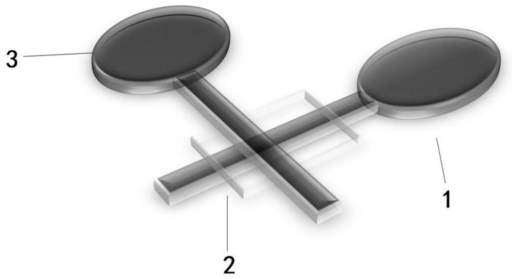
[0037] Such as figure 1 As shown, the present embodiment provides a memristor, and its preparation method is as follows:

[0038] (1) 36mg carboxylated chitosan, 24mg polyvinyl alcohol (PVA) and 40mg ammonium nitrate (NH 4 NO 3 ) was dissolved in 10mL deionized water to obtain the resistive layer material;

[0039] (2) Forming a W electrode 1 with a thickness of 50 nm on the glass substrate by a sputtering process;

[0040] (3) Spin-coat the resistive layer material prepared in step (1) on the W electrode 1 prepared in step (2) to form a resistive layer 2 with a thickness of 200 nm;

[0041] (4) An Ag electrode 3 with a thickness of 50 nm is formed on the resistive layer 2 prepared in step (3) by using an electron beam evaporation process to obtain a memristor.

Embodiment 2

[0043] Such as figure 1 As shown, the present embodiment provides a memristor, and its preparation method is as follows:

[0044] (1) 48mg carboxylated chitosan, 12mg polyvinyl alcohol (PVA) and 40mg ammonium nitrate (NH 4 NO 3 ) was dissolved in 10ml deionized water to obtain the resistive layer material;

[0045] (2) Forming a W electrode 1 with a thickness of 100 nm on a glass substrate by a sputtering process;

[0046] (3) Spin-coat the resistive layer material prepared in step (1) on the W electrode 1 prepared in step (2) to form a resistive layer 2 with a thickness of 500 nm;

[0047] (4) An Ag electrode 3 with a thickness of 100 nm is formed on the resistive layer 2 prepared in step (3) by using an electron beam evaporation process to obtain a memristor.

experiment example

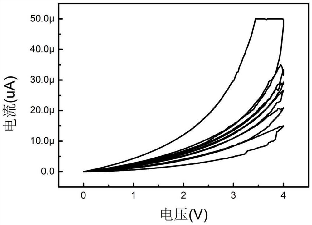
[0049] Such as figure 2 As shown, using the Agilent B1500A semiconductor tester, the W electrode is grounded, the Ag electrode is connected to the positive electrode, and a voltage of 4V is applied to the device for scanning test. As the number of scans continues to increase, it can be found that the current is constantly increasing and the conductance is constantly changing. , the resistance of the resistive layer keeps decreasing.

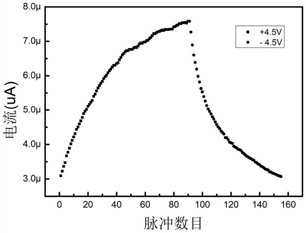
[0050] Such as image 3 As shown, using the Keithley 2636B semiconductor tester to apply 90 consecutive positive pulse voltages of 4.5V to the device, the read voltage of 0.5V (pulse interval is 60ms) is limited to 500uA, and the conductance of the device gradually increases from 3uA to 7.5 uA, continuous application of 80 reverse -4.5V pulse voltages, -0.5V read voltage (pulse interval 60ms), the conductance of the device dropped from 7.5uA to 3uA.

[0051] Such as Figure 4As shown, using Keithley 2636B semiconductor tester to apply 400 con...


PUM

PropertyMeasurementUnit
thicknessaaaaaaaaaa
thicknessaaaaaaaaaa
thicknessaaaaaaaaaa

Abstract

The invention provides a resistive layer material, a memristor and a preparation method thereof, and relates to the field of electronic devices. The resistive layer material comprises carboxylated chitosan, polyvinyl alcohol and ammonium nitrate. A resistive layer formed from the resistive layer material is applied to the memristor. The resistance state can be slowly changed through the binding effect of the polymer on metal ions to achieve enhanced suppression of pulses instead of being changed from a high resistance state to a low resistance state instantly. After the pulse is applied, the conductance state is changed by two orders of magnitude, and current limiting cannot be achieved. Excellent synaptic plasticity such as excitatory post-synaptic current and inhibitory post-synaptic current can be achieved. The resistive layer material has very good application value in a brain-like memristive device in the future, which is indispensable for synaptic computation and information storage.

Description

technical field [0001] The invention relates to the field of electronic devices, in particular to a resistive layer material, a memristor and a preparation method thereof. Background technique [0002] The rapid development of electronic technology and information science has put forward requirements for various types of device structures, materials and calculation methods. Memory devices are one of the most important components in electronic devices, especially memristor-based memories have potential applications in next-generation information technology. Memristors with a metal-insulator-metal structure offer significant advantages such as structural simplicity, nonvolatile storage, and continuous analog resistance switching through an insulator layer for computation. Among them, redox-based resistive-switching memristors are considered to be one of the most promising devices in future non-volatile memory technologies due to their high operating speed, low power consumpti...

Claims


Application Information

Patent Timeline
Patent Type & Authority Applications(China)
IPC IPC(8): H01L45/00
CPCH10N70/841H10N70/881H10N70/023Y02D10/00
Inventor 王琦王正鲜林燕贺德衍
Owner LANZHOU UNIVERSITY
Why Eureka
Try Eureka