Welding method and chip packaging method

A welding method and welding part technology, applied in the direction of assembling printed circuits, printed circuits, electrical components, etc. with electrical components, can solve the problems of high melting point of the surface oxide film, affecting product reliability, affecting product heat dissipation performance and other problems

Pending Publication Date: 2021-09-10
SUZHOU TF AMD SEMICON CO LTD
View PDF6 Cites 0 Cited by
  • Summary
  • Abstract
  • Description
  • Claims
  • Application Information

AI Technical Summary

Problems solved by technology

[0003] At present, metal sheets, such as indium sheets, tin-silver sheets or other metal sheets, are usually used. In order to ensure the connection between the metal layer and the chip and the heat dissipation cover, it is necessary to use resin flux to remove the oxide on the surface of the metal sheet to complete the welding. However, currently The metal sheet is easily oxidized, and the oxide film on its surface has a high melting point. Flux must be used to remove the oxide film to achieve the soldering effect. Since the flux residue cannot be removed by cleaning, the flux residue will remain between the heat dissipation cover and the chip. The use of subsequent products may cause product failure, and the resin flux will cause metal splashes due to its volatilization during the heating process, resulting in short circuit of the surrounding capacitors and chips, which will affect the reliability of the product; and resin flux in The gas volatilized during the heating process will form cavities in the metal layer, which will affect the heat dissipation performance of the product

Method used


Image

  • Welding method and chip packaging method
  • Welding method and chip packaging method
  • Welding method and chip packaging method

Examples


Embodiment Construction

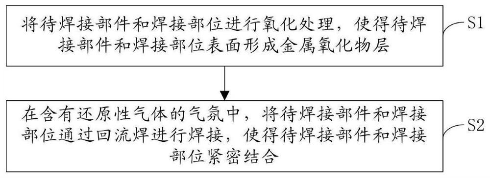
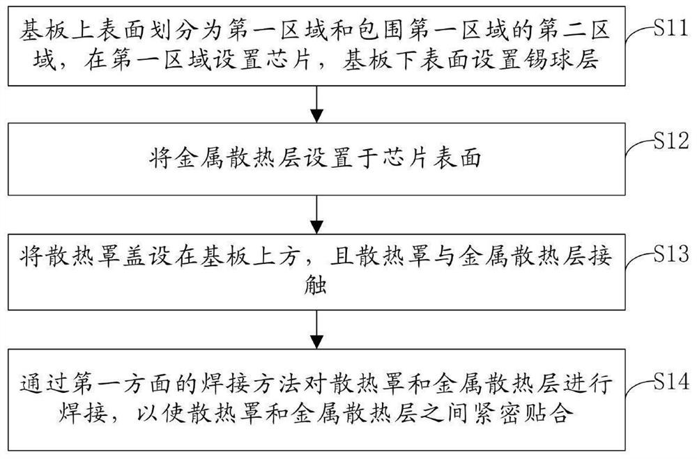
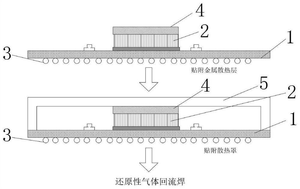
[0034] The application will be further described in detail below in conjunction with the accompanying drawings and embodiments. It should be understood that the specific embodiments described here are only used to explain related inventions, rather than to limit the invention. It should also be noted that, for ease of description, only parts related to the invention are shown in the drawings.

[0035] It should be noted that, in the case of no conflict, the embodiments in the present application and the features in the embodiments can be combined with each other. The present application will be described in detail below with reference to the accompanying drawings and embodiments.

[0036] It should be noted that in the description of this application, the terms "first", "second" and so on are used for descriptive purposes only, and cannot be understood as indicating or implying relative importance or implicitly indicating the number of indicated technical features . Thus, t...


PUM

PropertyMeasurementUnit
melting pointaaaaaaaaaa

Abstract

The invention discloses a welding method and a chip packaging method, which are suitable for semiconductor packaging. The welding method comprises the steps: carrying out oxidation treatment on a to-be-welded component and a welding part, and enabling the surface of the to-be-welded component and the surface of the welding part to form a metal oxide layer; and in an atmosphere containing reducing gas, welding the to-be-welded component and the welding part through reflow soldering, so that the to-be-welded component and the welding part are tightly combined. According to the welding method, the oxide on the surfaces of the to-be-welded component and the welding part is subjected to the reduction reaction in the heating process by using the reducing gas, so that reliable welding of the metal heat dissipation layer is guaranteed, and the problem that the yield of chips is low due to the fact that resin scaling powder is used in the prior art is effectively solved.

Description

technical field [0001] The invention generally relates to the technical field of semiconductor testing, and in particular to a welding method and a chip packaging method. Background technique [0002] With the continuous development and progress of the integrated circuit industry, the monolithic integration of chips is getting higher and higher, power consumption is getting bigger and bigger, and the requirements for packaging technology are getting higher and higher. At present, in order to improve the heat dissipation performance in the chip packaging process, a metal layer is generally provided on the chip and the heat dissipation cover, which is beneficial to heat dissipation on the one hand, and is beneficial to the connection between the heat dissipation cover and the chip on the other hand. [0003] At present, metal sheets, such as indium sheets, tin-silver sheets or other metal sheets, are usually used. In order to ensure the connection between the metal layer and t...

Claims


Application Information

Patent Timeline
Patent Type & Authority Applications(China)
IPC IPC(8): H01L21/50H01L21/56H05K3/34
CPCH01L21/50H01L21/56H05K3/3494
Inventor 周云曾昭孔黄柏荣卢玉溪
Owner SUZHOU TF AMD SEMICON CO LTD
Why Eureka
Try Eureka