

Method for manufacturing pre-cut SDB FinFET
A manufacturing method and a part of the technology, applied in the direction of semiconductor/solid-state device manufacturing, electrical components, circuits, etc., can solve problems such as device performance degradation
Pending Publication Date: 2021-09-14
SHANGHAI HUALI INTEGRATED CIRCUTE MFG CO LTD
View PDF0 Cites 0 Cited by
- Summary
- Abstract
- Description
- Claims
- Application Information
AI Technical Summary
Problems solved by technology
[0006] In view of the above-mentioned shortcomings of the prior art, the purpose of the present invention is to provide a method for manufacturing SDB FinFET first, which is used to solve the problem that the pressure of the metal gate and the tungsten electrode reacts on SiGe or SiP in the SDB first-cut process in the prior art. The problem that the pressure leads to the degradation of the performance of the device
Method used
View moreImage
Smart ImageViewing Examples

Examples
Embodiment Construction
[0045] The embodiments of the present invention will be easily understood by those skilled in the
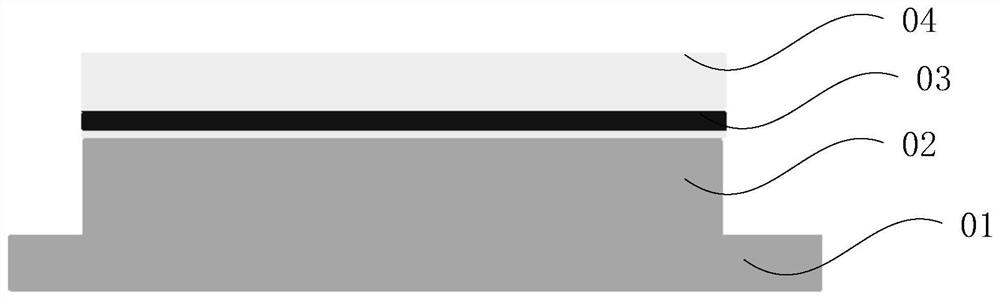
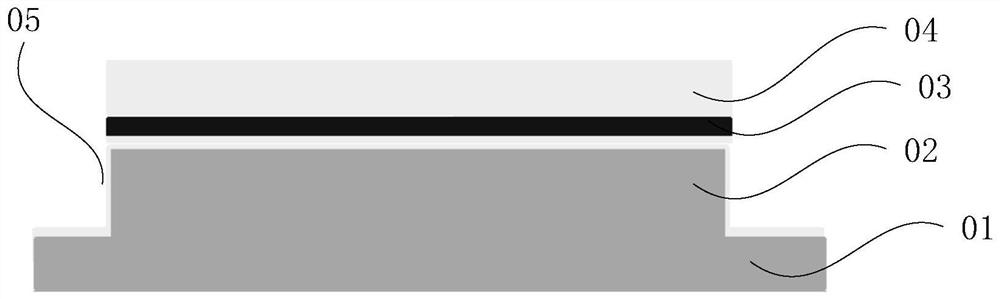
[0046] See Figures 2 to 16 . It should be noted that the illustrations provided in the present embodiment will illustrate the basic contemplation of the present invention in a schematic manner, and only the components, shapes, shapes, shapes, shapes related to the components of the present invention are displayed in the pattern rather than in accordance with the actual implementation. Dimensions, the type, quantity, and proportion of each component can be a random change in the actual implementation, and its component layout is also more complicated.
[0047] The present invention provides ...
Login to View More PUM
 Abstract
The invention provides a method for manufacturing a pre-cut SDB FinFET. The method comprises the steps of: forming a plurality of fin structures which are arranged at intervals in the longitudinal direction, and etching the fin structures to form SDB grooves; depositing a dielectric layer to fill the SDB grooves; performing etching to expose the upper ends of the fin structures and a part of the upper end of each SDB groove; forming a plurality of dummy gates and side walls of the dummy gates, which are arranged at intervals along the transverse direction, on the fin structures and the SDB grooves; forming a SiP epitaxial structure and a SiGe epitaxial structure on the fin structure between the two adjacent dummy gates on the two sides of each SDB groove respectively; removing other dummy gates except the dummy gates on the SDB grooves to form grooves; and filling HK metal in the grooves where the dummy gates are removed to form HK metal gates. According to the method of the invention, the polycrystalline silicon of the SDB is reserved, so that the pressure release risk of the SiP epitaxial layer and the SiGe epitaxial layer is reduced; and the SDB grooves are not filled with the HK metal gates, so that the pressure of HKK metal layers does not interact with the pressure of the epitaxial layer, and the performance of the device is improved.
Description
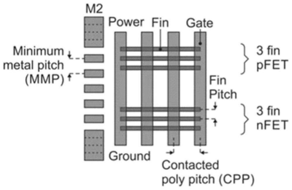
Technical field [0001] The present invention relates to the field of semiconductor technology, and more particularly to a method of manufacturing a first-cut SDB FinFET. Background technique [0002] The logic design in the logical standard unit is created using standard units. The height of the unit is measured by the track number by metal spacing (PITCH), orbit and PITCH. figure 1 One half of the 7.5 track unit is shown, the power supply (POWER), and the level rail is located in the upper unit and the unit below. [0003] The unit width is related to the CONTACT POLY PITCH, CPP), and the number of CPPs in the width of the constituent unit depends on the unit type and whether the unit has a dual diffusion interruption (DDB) or single diffusion interruption (SDB). [0004] A DDB adds a half CPP on each side of the unit. For actual units, such as NAND gates and unit scan triggers, the number of CPPs on the unit width is large, and the SDB has a small amount of DDB. [0005] In the...
Claims
Login to View More Application Information
Patent Timeline
 Patent Type & AuthorityApplications(China)
IPC IPC(8): H01L21/336H01L29/78
CPCH01L29/785H01L29/66795
Inventor李勇
OwnerSHANGHAI HUALI INTEGRATED CIRCUTE MFG CO LTD