
Planarization etchback method after groove is filled with medium

A trench filling and planarization technology, used in electrical components, circuits, semiconductor/solid-state device manufacturing, etc., can solve the problems of metal voids affecting the yield of silicon-based surface, increasing metal contact resistance, and poor uniformity. Follow-up process defects, reduce height difference, good uniformity

Active Publication Date: 2021-09-17
XIAN MICROELECTRONICS TECH INST
View PDF11 Cites 0 Cited by
  • Summary
  • Abstract
  • Description
  • Claims
  • Application Information

AI Technical Summary

Problems solved by technology

The unevenness of the dielectric on the surface of the trench will lead to increased metal contact resistance in subsequent processes, and even metal voids will affect the yield of the silicon-based surface
[0003]Traditional and existing technologies use chemical mechanical polishing for dielectric planarization after trench filling. This method is expensive and has poor uniformity

Method used


Image

  • Planarization etchback method after groove is filled with medium
  • Planarization etchback method after groove is filled with medium
  • Planarization etchback method after groove is filled with medium

Examples


Embodiment 1

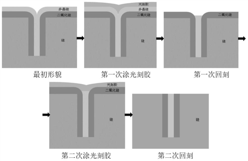
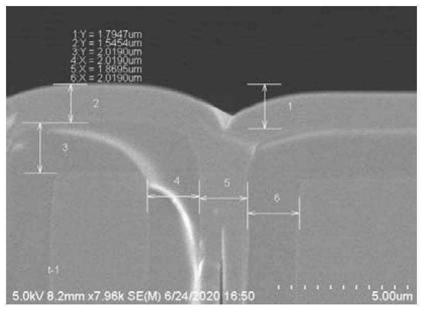
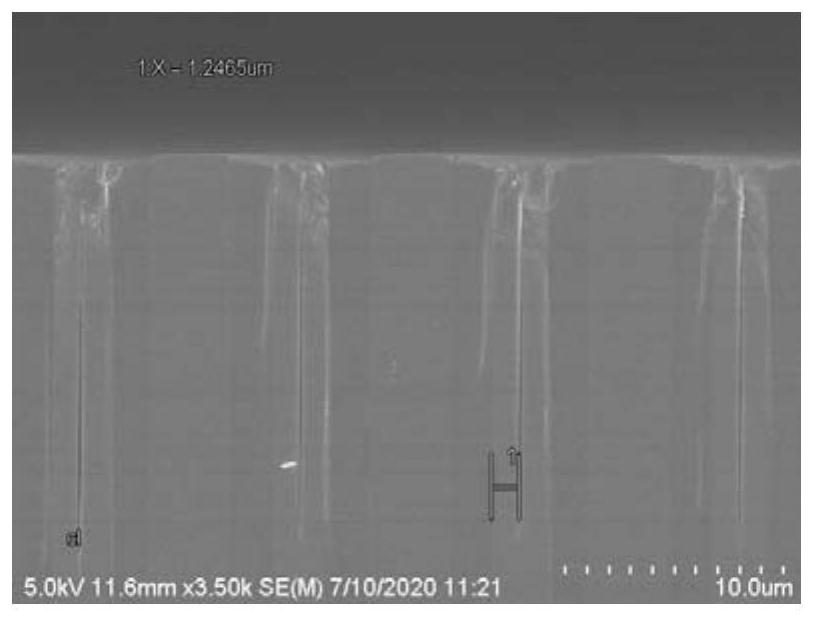
[0039] Such as figure 2 As shown, a 6-inch silicon wafer is selected, and a 2.0 μm thick silicon dioxide layer is grown in the silicon wafer groove first, and then a 1.5 μm thick polysilicon layer is filled. After filling, the thickness of the polysilicon layer on the surface of the silicon wafer is 1.5μm, the thickness of the silicon dioxide layer is 2.0μm, the first photoresist coating is performed, and the thickness of the photoresist is After the surface is planarized, the first etching is carried out, using AMAT CENTURA5200 polysilicon etching machine, the pressure is 4mTorr, the Source power is 475W, and the Bias power is 100W; the etching gas is HBr and Cl 2 and HeO 2 , where the flow rate of HBr is 20sccm, Cl 2 The flow rate is 68sccm, HeO 2 The flow rate of the polysilicon layer is 2sccm, and the etching rate of the polysilicon layer is / min, the etching rate of the photoresist layer is / min, remove all the photoresist layer and polysilicon layer on the top o...


PUM


Abstract

The invention provides a planarization etchback method after a groove is filled with a medium, which comprises the following specific steps of: filling a double-layer dielectric in the groove on the surface of a silicon substrate, forming a first dielectric layer and a second dielectric layer on the surface of the silicon substrate from top to bottom, and coating photoresist on the first dielectric layer for the first time; etching the photoresist and the first dielectric layer, completely etching the photoresist on the surface of the silicon substrate after etching, wherein the first dielectric layer with a certain height is left on the top of the groove in the surface of the silicon substrate; after the treatment, carrying out photoresist coating on the second dielectric layer on the surface of the silicon substrate for the second time; adjusting the selection ratio of the photoresist to the first medium and the second medium, completely etching the second medium layer, the photoresist coated for the second time and the remaining first medium layer at the same time. By means of the planarization back-etching method, the flatness of the surface of the groove in the silicon substrate after medium etching can be remarkably improved, the machining quality is improved, and subsequent process defects are reduced.

Description

technical field [0001] The invention belongs to the technical field of semiconductors, in particular to a method for planarizing and etching back after a trench is filled with a medium. Background technique [0002] At present, deep trench structure devices are widely used in semiconductor technology, such as electronic devices that use deep trench structures for electrical insulation, and power MOSFETs that use super junction technology as high-voltage switching converters, etc., are widely used in mobile communications and control circuits , Automotive electronics, etc. The unevenness of the dielectric on the trench surface will lead to increased metal contact resistance in subsequent processes, and even metal voids will affect the yield of the silicon-based surface. [0003] The traditional and existing technologies use a chemical mechanical polishing method for dielectric planarization after trench filling, which is expensive and has poor uniformity. Contents of the i...

Claims


Application Information

Patent Timeline
IPC IPC(8): H01L21/027H01L21/311
CPCH01L21/0274H01L21/31116H01L21/31138H01L21/31144
Inventor 王一义曾坤郝军代鹏昊李林刘存生
Owner XIAN MICROELECTRONICS TECH INST
Learn More