IGBT device, preparation method thereof and electronic product

A technology for electronic products and devices, applied in the field of IGBT devices and their preparation, can solve the problems of large on-voltage drop and weak anti-latch ability, and achieve the advantages of reducing on-voltage drop, improving quality, and improving anti-latch ability. Effect

Pending Publication Date: 2021-09-21
GUANGDONG MIDEA WHITE HOME APPLIANCE TECH INNOVATION CENT CO LTD +1
View PDF5 Cites 0 Cited by
  • Summary
  • Abstract
  • Description
  • Claims
  • Application Information

AI Technical Summary

Problems solved by technology

[0004] The present invention at least solves the technical problems of weak latch-up resistance and large turn-on voltage drop of IGBT devices in the related art to a certain extent. Therefore, the present invention provides an IGBT device and its preparation method and electronic products

Method used


Image

  • IGBT device, preparation method thereof and electronic product
  • IGBT device, preparation method thereof and electronic product
  • IGBT device, preparation method thereof and electronic product

Examples


Embodiment approach

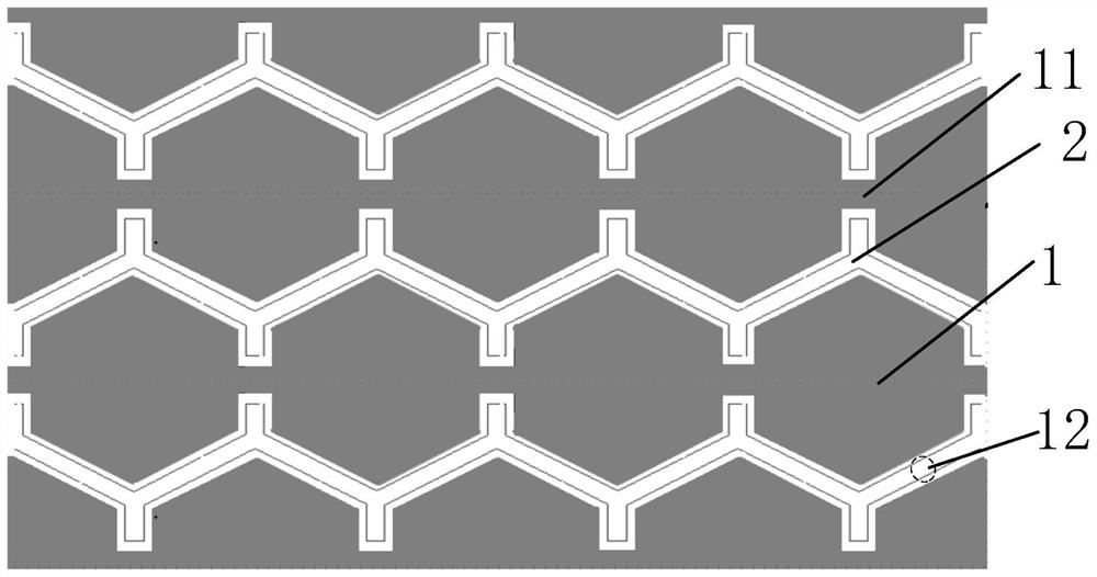
[0042] In some embodiments, the gate array includes multiple rows of gates 1 . Wherein, each gate 1 in each row of gates 1 is arranged on the same straight line, and the number of gates included in each row of gates 1 is set according to the actual function of the IGBT device, and the adjacent rows of gates in the gate array are in phase with each other. Embedded setting, so as to be able to reduce the interval area between each gate 1, and then, can reduce the setting area of ​​the emitter source region 3 and the first body region 4, so as to increase the layout density of the gate array, and realize the cell Compact distribution.

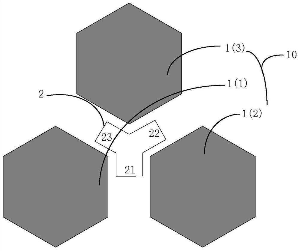
[0043] In the embodiment of the present invention, the interval width between each adjacent gate 1 in the gate array can be the same, and the interval width between any two adjacent gates 1 is smaller than the surface shape of the gate 1, Strip-shaped emitter electrodes 2 with a smaller width than the gate 1 can be provided in the spaced area to ...


PUM


Abstract

The invention discloses an IGBT device, a preparation method thereof and an electronic product, and belongs to the technical field of integrated circuits. A cellular region of the IGBT device comprises a grid array; emitter electrodes are arranged in interval areas between grids of the grid array, so that the multiple emitter electrodes can surround the same grid; an emitter source region and a first body area in contact with the emitter source region are formed below each emitter electrode; and the contact area of the emitter source region and the first body region is distributed along the arrangement direction of the emitter electrode. According to the invention, the technical problems of weak latch-up resistance and large conduction voltage drop of the IGBT device are solved.

Description

technical field [0001] The invention belongs to the technical field of integrated circuits, and in particular relates to an IGBT device, a preparation method thereof and electronic products. Background technique [0002] Insulated Gate Bipolar Transistor (Insulated Gate Bipolar Transistor, referred to as IGBT) is a composite full-control voltage drive composed of BJT (Bipolar Junction Transistor, bipolar transistor) and MOSFET (Metal Oxide Semiconductor Field-Effect, metal oxide half field-effect transistor Transistor) Power semiconductor devices, both MOSFET (Metal-Oxide Semiconductor Field-Effect Transistor, referred to as Metal-Oxide-Semiconductor Field-Effect Transistor, MOSFET) device high input impedance and power transistor (ie giant Transistor (GTR for short) has two advantages of low conduction voltage drop. Because IGBT has the advantages of small driving power and low saturation voltage, IGBT as a new type of power electronic device is widely used in the fields o...

Claims


Application Information

Patent Timeline
Patent Type & Authority Applications(China)
IPC IPC(8): H01L29/739H01L29/06H01L29/423H01L21/331
CPCH01L29/7393H01L29/0603H01L29/0684H01L29/66325H01L29/42356
Inventor 兰昊
Owner GUANGDONG MIDEA WHITE HOME APPLIANCE TECH INNOVATION CENT CO LTD
Why Eureka
Try Eureka