Semiconductor structure and forming method thereof

A technology of semiconductor and channel structure, applied in semiconductor devices, semiconductor/solid-state device manufacturing, transistors, etc., can solve the problems of poor overall performance of semiconductor devices, improve surface utilization, improve carrier mobility, and improve integration degree of effect

Pending Publication Date: 2021-10-12
SEMICON MFG INT (SHANGHAI) CORP +1
View PDF0 Cites 0 Cited by
  • Summary
  • Abstract
  • Description
  • Claims
  • Application Information

AI Technical Summary

Problems solved by technology

[0004] However, the performance of the SRAM in the semiconductor device formed in the prior art needs to be further improved, so that the overall performance of the semiconductor device is poor

Method used


Image

  • Semiconductor structure and forming method thereof
  • Semiconductor structure and forming method thereof
  • Semiconductor structure and forming method thereof

Examples


Embodiment Construction

[0013] Currently formed devices still suffer from poor performance. The reasons for the poor performance of the device are analyzed in conjunction with a method of forming a semiconductor structure.

[0014] refer to Figure 1 to Figure 4 It is a structural schematic diagram corresponding to each step in a method for forming a semiconductor structure.

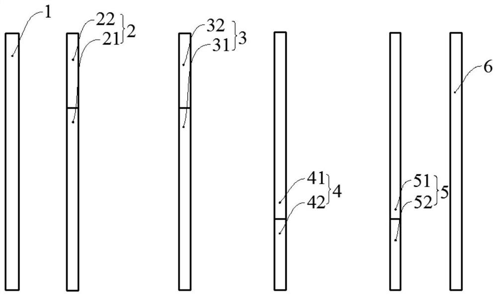
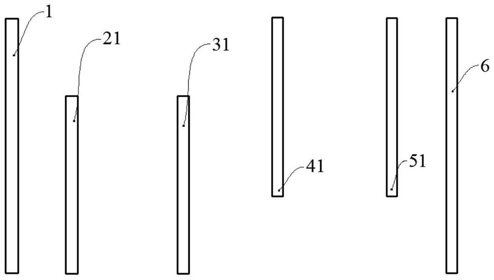
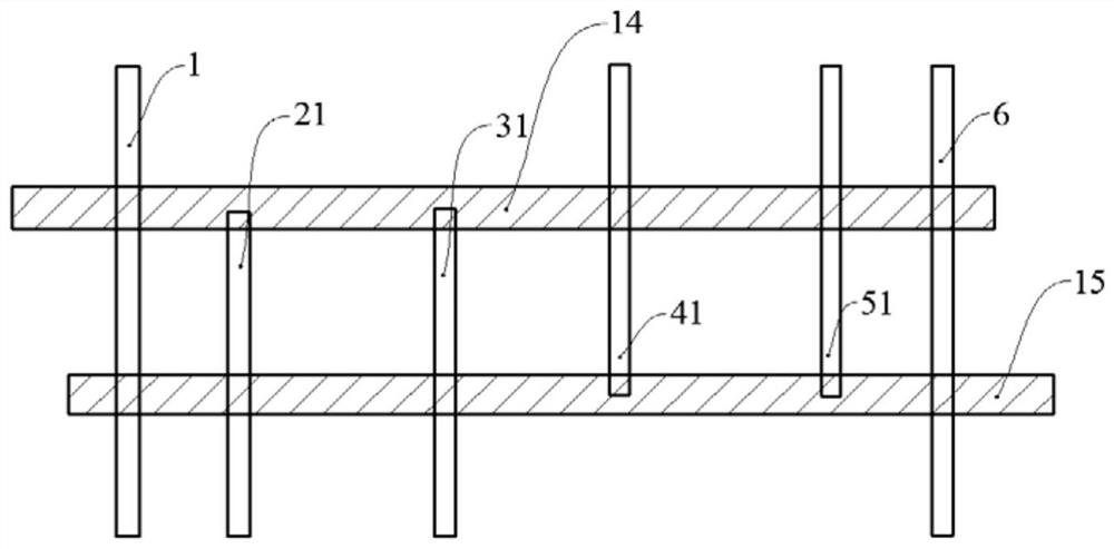
[0015] Such as figure 1 As shown, a base is provided, and the base includes a substrate (not shown in the figure) and six discrete fins located on the substrate, the fins extend in the longitudinal direction, and the first fins in the transverse direction 1. The second fin 2 , the third fin 3 , the fourth fin 4 , the fifth fin 5 and the sixth fin 6 , the second fin 2 is symmetrical to the fifth fin 5 , The third fin 3 is centrally symmetrical to the fourth fin 4, the first fin 1 includes a first device fin, and the second fin 2 includes a second device fin 21 and a second dummy fin 22. The third fin 3 includes the third dev...


PUM

PropertyMeasurementUnit
widthaaaaaaaaaa
widthaaaaaaaaaa

Abstract

The invention discloses a semiconductor structure and a forming method thereof, and the method comprises the steps: a substrate which comprises a first region, and the first region comprises a first longitudinal region and a second longitudinal region which are adjacent in the longitudinal direction; a channel body which is located on the substrate, the channel body extends in the longitudinal direction, wherein the channel body comprises a first channel part and a second channel part in the longitudinal direction, the transverse width of the first channel part is larger than that of the second channel part, the transverse direction is perpendicular to the longitudinal direction, in the first region, the first channel part is located in the first longitudinal region, and the second channel part is located in the second longitudinal region; a first gate structure across the first channel feature; and a second gate structure across the second channel feature. According to the embodiment of the invention, by increasing the transverse width of the first channel component, the carrier mobility in the pull-down transistor is improved, the surface utilization rate of the semiconductor structure is improved, and the integration level of the semiconductor structure is correspondingly improved.

Description

technical field [0001] Embodiments of the present invention relate to the field of semiconductor manufacturing, and in particular, to a semiconductor structure and a method for forming the same. Background technique [0002] In the current semiconductor industry, integrated circuit products can be mainly divided into three types: logic, memory and analog circuits, among which memory devices account for a considerable proportion of integrated circuit products. With the development of semiconductor technology, storage devices are more widely used, and the storage device and other device regions need to be formed on a chip at the same time to form an embedded semiconductor storage device. For example, to embed the storage device in the central processing unit, it is necessary to make the storage device compatible with the embedded central processing unit platform, and maintain the specifications and corresponding electrical performance of the original storage device. [0003] ...

Claims


Application Information

Patent Timeline
Patent Type & Authority Applications(China)
IPC IPC(8): H01L27/11H01L21/8244
CPCH10B10/12
Inventor 王楠
Owner SEMICON MFG INT (SHANGHAI) CORP
Why Eureka
Try Eureka