

Semiconductor device and related manufacturing method
A manufacturing method and semiconductor technology, applied in the fields of semiconductor devices, semiconductor/solid-state device manufacturing, electrical components, etc., can solve the problems of increasing device area, increasing the cost of a single chip, intensifying the lateral diffusion of impurities, etc., achieving low annealing thermal budget, The effect of improving surface utilization and reducing annealing time
- Summary
- Abstract
- Description
- Claims
- Application Information
AI Technical Summary
Problems solved by technology
Method used
Image

Examples
Embodiment Construction
[0039] Various embodiments of the invention will be described in more detail below with reference to the accompanying drawings. In the various drawings, the same elements are denoted by the same or similar reference numerals. For the sake of clarity, various parts in the drawings have not been drawn to scale.
[0040] The specific implementation manners of the present invention will be further described in detail below in conjunction with the accompanying drawings and embodiments.
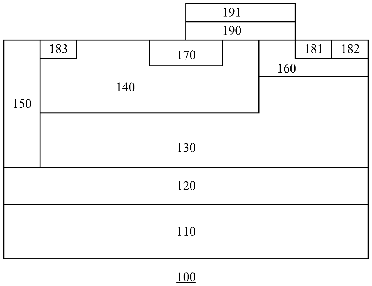
[0041] figure 1 A schematic device cross-sectional structure schematic diagram showing a process schematic of a semiconductor device according to the prior art. As shown in the figure, a semiconductor device 100 in the prior art includes a substrate 110, a buried layer 120, an epitaxial layer 130, a drift region 140, an isolation region 150, a well region 160, a shallow trench isolation region 170, a first doped region 181 , a second doped region 182 , a third doped region 183 , a gate oxide lay...
PUM
 Abstract
Description
Claims
Application Information