Four-dimensional high-temporal-spatial-resolution ultrafast photon electron multimode detection device

A space-time resolution and detection device technology, which is applied in measuring devices, analyzing materials, and using wave/particle radiation for material analysis, etc., can solve the problems of inability to detect processing results, inability to observe ultrafast laser dynamic processes, etc., and achieve high precision and high Continuity detection function, extended observation capability, improved reliability and stability effects

Inactive Publication Date: 2021-10-29
BEIJING INSTITUTE OF TECHNOLOGYGY
View PDF9 Cites 1 Cited by
  • Summary
  • Abstract
  • Description
  • Claims
  • Application Information

AI Technical Summary

Problems solved by technology

[0003] The purpose of the present invention is to solve the problem that the dynamic process of ultrafast lasers cannot be observed in the prior art, and thus the processing results cannot be detected, and to provide a four-dimensional high-time-space

Method used


Image

  • Four-dimensional high-temporal-spatial-resolution ultrafast photon electron multimode detection device
  • Four-dimensional high-temporal-spatial-resolution ultrafast photon electron multimode detection device

Examples


Embodiment 1

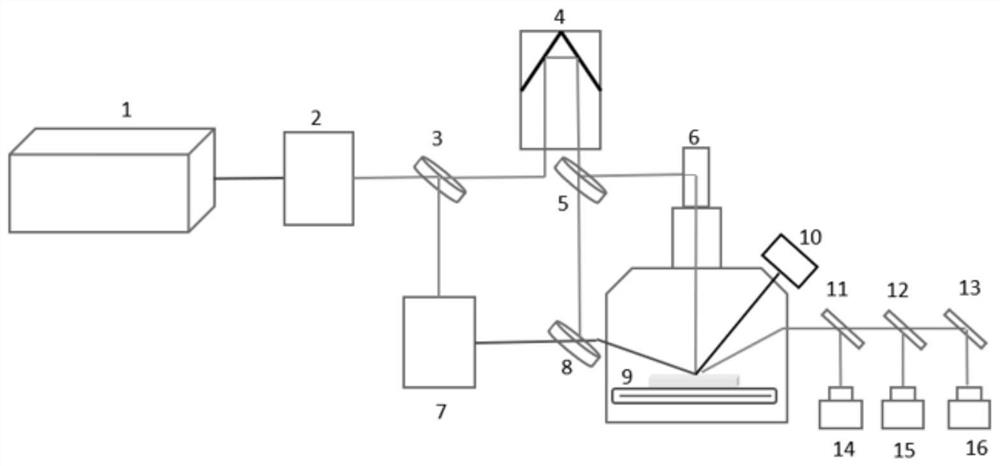
[0030] On a CdSe thin film sample with a thickness of 500 μm, a four-dimensional high-spatial-resolution ultrafast photonic electron multi-mode detection device was used to study its carrier dynamics and the dynamic change process of electron density during processing.

[0031] The working process is as follows,

[0032] Step 1. Place the selected Si sample on the sample stage.

[0033] Step 2, as attached figure 1 As shown, the optical path of the femtosecond laser system 1 is adjusted, and the basic output of the ultrafast femtosecond laser is passed through a double frequency crystal to generate a 515nm laser, which is then divided into two paths by the first beam splitter 31:1, and one path is used as the pumping light. All the way as a probe light.

[0034] Step 3: The pump light is focused onto the sample 9 through the frequency-tripling crystal 7 and the beam combiner 8, and the pump light is adjusted to accurately enter the center of the sample 9 at an angle of 50 de...


PUM


Abstract

The invention relates to a four-dimensional high-temporal-spatial-resolution ultrafast photon electron multimode detection device, and belongs to the field of laser micro-nano machining and material science application. According to the invention, through a pumping detection technology, focused photons from femtosecond to picosecond are accurately focused to a micro-nano scale sample, and detection is carried out through organic combination of an ultrafast scanning electron microscope and a CCD; a cooling filament is excited by ultrafast laser to form an ultrafast electron beam for observation; the CCD is irradiated by ultrafast laser for observation, so that multimode detection of ultrafast electrons and ultrafast photons can be realized at the same time; detection electrons can be regulated and controlled, so that the detection electrons and photons jointly act on a sample, and multi-mode ultrafast observation of the synergistic effect process of the electrons and the photons is realized; and micro-nano structure processing or modification can be carried out on a sample, and in-situ measurement processing or modified ultrafast carrier dynamics research can be carried out.

Description

technical field [0001] The invention relates to a four-dimensional high-time-space resolution ultrafast photon electronic multi-mode detection device, which belongs to the field of laser micro-nano processing and material science applications. Background technique [0002] The study of ultrafast dynamics to explore the microstructure of matter and the process of physical and chemical transient changes has opened up new development directions for different disciplines, especially in the field of ultrafast laser manufacturing. Ultrafast laser has the characteristics of ultra-powerful, ultra-fast, and ultra-precise, and is one of the frontiers and important growth points of manufacturing technology. Through the interaction between laser and materials, changing the state and properties of materials, and realizing shape control from micron to nanoscale or across scales, has attracted much attention for many years. The interaction between femtosecond laser and material is a nonli...

Claims


Application Information

Patent Timeline
IPC IPC(8): G01N23/2251G01N23/227G01N23/2208
CPCG01N23/2251G01N23/227G01N23/2208G01N2223/072G01N2223/084G01N2223/073G01N2223/102
Inventor 姜澜孙靖雅郭宝山
Owner BEIJING INSTITUTE OF TECHNOLOGYGY
Why Eureka
Try Eureka