Cyclic conversion SAR ADC circuit and SAR ADC method
A circuit, digital-to-analog conversion technology, applied in the field of cyclic conversion SARADC circuits, can solve the problems of comparator noise accuracy and speed, and achieve the effect of reducing the number of capacitors, the total area of the capacitors, and meeting high-precision matching requirements
- Summary
- Abstract
- Description
- Claims
- Application Information
AI Technical Summary
Problems solved by technology
Method used
Image
Examples
Embodiment 1
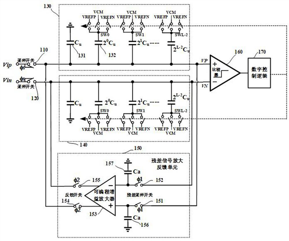
[0040] like figure 1 As shown, this embodiment provides a cyclic conversion SAR ADC circuit, including: a first sampling switch 110, a second sampling switch 120, a first digital-to-analog conversion unit 130, a second digital-to-analog conversion unit 140, a residual signal amplification feedback Unit 150, comparator 160 and SAR control logic unit 170, wherein:
[0041] The first sampling switch 110 is used to receive the positive terminal input of the differential signal;
[0042] The second sampling switch 120 is used to receive the negative terminal input of the differential signal;
[0043] The first digital-to-analog conversion unit 130 is connected to the first output end of the first sampling switch 110 and the residual signal amplification feedback unit 150 for digital-to-analog conversion;
[0044] The second digital-to-analog conversion unit 140 is connected to the second sampling switch 120 and the second output end of the residual signal amplification feedback u...
Embodiment 2
[0057] This embodiment provides a SAR ADC method. The SAR ADC method is implemented based on the SAR ADC cyclic conversion circuit provided in Embodiment 1, and at least includes:
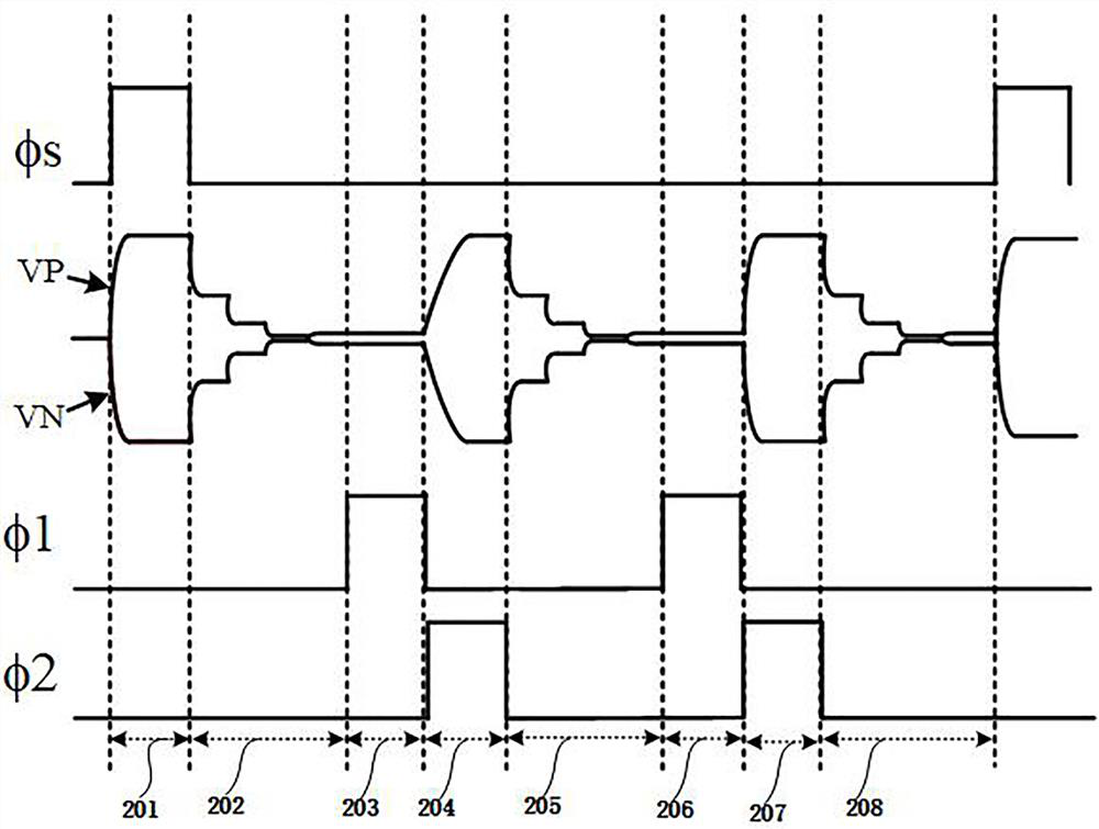
[0058] Step S1: if figure 1 and figure 2 As shown, based on the first sampling switch 110 and the second sampling switch 120, the differential signal is sampled to the first digital-to-analog conversion unit 130 and the second digital-to-analog conversion unit 140, that is figure 2 In the process 201 of sampling the differential signal, and then performing successive approximation conversion, that is figure 2 In the process 202 of successive approximation of the difference signal, the first group of digital signals is output, and the first residual signal is obtained at the same time.
[0059] Step S2: if figure 1 and figure 2 As shown, the first residual signal is sampled based on the first residual sampling switch 151 and the second residual sampling switch 152, namely figure 2 In the p...
PUM
 Abstract
Description
Claims
Application Information

