In-memory logic circuit

A logic circuit and logic input technology, which is applied in the field of semiconductors, can solve the problems of high hardware resource overhead and slow working time, and achieve the effects of low logic operation steps, saving time and waste, and saving circuit area overhead

Pending Publication Date: 2021-11-02
PEKING UNIV
View PDF0 Cites 1 Cited by
  • Summary
  • Abstract
  • Description
  • Claims
  • Application Information

AI Technical Summary

Problems solved by technology

[0003] However, in-memory logic circuits based on non-volatile memory in the prior art often require a large number of auxiliary memory units and multiple cycles for memory writing, which makes the additional overhead of hardware resources too large and the working time slow

Method used


Image

  • In-memory logic circuit
  • In-memory logic circuit
  • In-memory logic circuit

Examples


Embodiment Construction

[0029] In order to make the purpose, technical solutions and advantages of the present invention clearer, the technical solutions in the present invention will be clearly and completely described below in conjunction with the accompanying drawings in the present invention. Obviously, the described embodiments are part of the embodiments of the present invention , but not all examples. Based on the embodiments of the present invention, all other embodiments obtained by persons of ordinary skill in the art without creative efforts fall within the protection scope of the present invention.

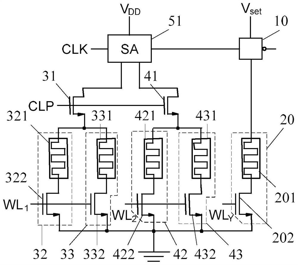
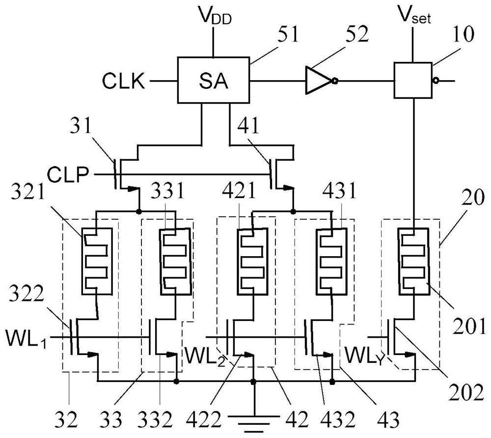
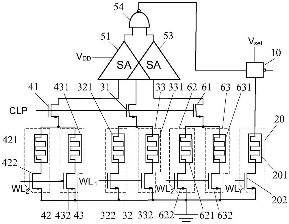
[0030] Combine below Figure 1-Figure 7 The in-memory logic circuit provided by the present invention is described.

[0031] figure 1 It is one of the circuit diagrams of the in-memory logic circuit provided by the present invention. Such as figure 1 As shown, the memory logic circuit includes: a logic input unit, a reference comparison unit, a logic processing unit, a CMOS transmission g...


PUM


Abstract

The invention provides an in-memory logic circuit. The in-memory logic circuit comprises a logic input unit, a reference comparison unit, a logic processing unit, a CMOS (Complementary Metal Oxide Semiconductor) transmission gate, a logic output transistor and a memory unit, the logic input unit includes a first NMOS transistor, a first logic input-transistor-first memory cell and a second logic input-transistor-first memory cell connected in parallel to a source terminal of the first NMOS transistor; the reference comparison unit comprises a second NMOS transistor, a first reference comparison transistor-memory unit and a second reference comparison transistor-memory unit; the drain ends of the first NMOS transistor and the second NMOS transistor are respectively connected with two input ends of the first current sensitive amplifier; the output end of the logic processing unit is connected with the control end of the CMOS transmission gate; the input end of the CMOS transmission gate receives a setting signal, and the output end of the CMOS transmission gate is connected with a logic output transistor and a memory unit.

Description

technical field [0001] The invention relates to the technical field of semiconductors, in particular to a memory logic circuit. Background technique [0002] In-memory logic circuits are a novel architecture that solves the von Neumann bottleneck and memory wall problems in computers. In the prior art, memories that realize the functions of in-memory logic circuits can be divided into volatile memories and nonvolatile memories, wherein volatile memories, such as Static Random Access Memory (SRAM, Static Random Access Memory), Dynamic Random Access Memory Access memory (DRAM, Dynamic Random Access Memory); non-volatile memory, such as Resistive Random Access Memory (RRAM, Resistive Random Access Memory), Phase Change Random Access Memory (PCRAM, Phase Change Random Access Memory), Magnetic Random Access Memory (MRAM , Magnetoresistive Random AccessMemory). The in-memory logic circuit based on the non-volatile memory has the following advantages: 1. Non-volatile after the lo...

Claims


Application Information

Patent Timeline
IPC IPC(8): G11C16/04G11C8/08G11C8/14
CPCG11C16/0483G11C8/08G11C8/14Y02D10/00
Inventor 刘力锋宋仕岳沈文生黄鹏康晋锋张兴
Owner PEKING UNIV
Why Eureka
Try Eureka