Check patentability & draft patents in minutes with Patsnap Eureka AI!

LED chip epitaxial structure and preparation method thereof

A technology of LED chip and epitaxial structure, which is applied in the direction of electrical components, circuits, semiconductor devices, etc., can solve the problems of mismatch, substrate and epitaxial structure thermal mismatch lattice, etc., and achieve the effect of improving crystal quality

Active Publication Date: 2021-11-02
XIAMEN SILAN ADVANCED COMPOUND SEMICON CO LTD
View PDF4 Cites 0 Cited by
  • Summary
  • Abstract
  • Description
  • Claims
  • Application Information

AI Technical Summary

Problems solved by technology

[0004] The purpose of the present invention is to provide an LED chip epitaxial structure and its preparation method to solve the thermal mismatch and lattice mismatch problems between the substrate and the epitaxial structure, and to prevent impurities in the substrate from entering the epitaxial structure, thereby obtaining high-quality epitaxial structure

Method used


Image

  • LED chip epitaxial structure and preparation method thereof
  • LED chip epitaxial structure and preparation method thereof
  • LED chip epitaxial structure and preparation method thereof

Examples


Embodiment Construction

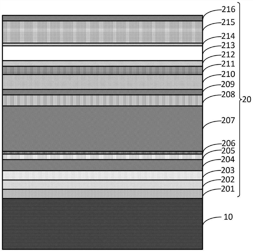
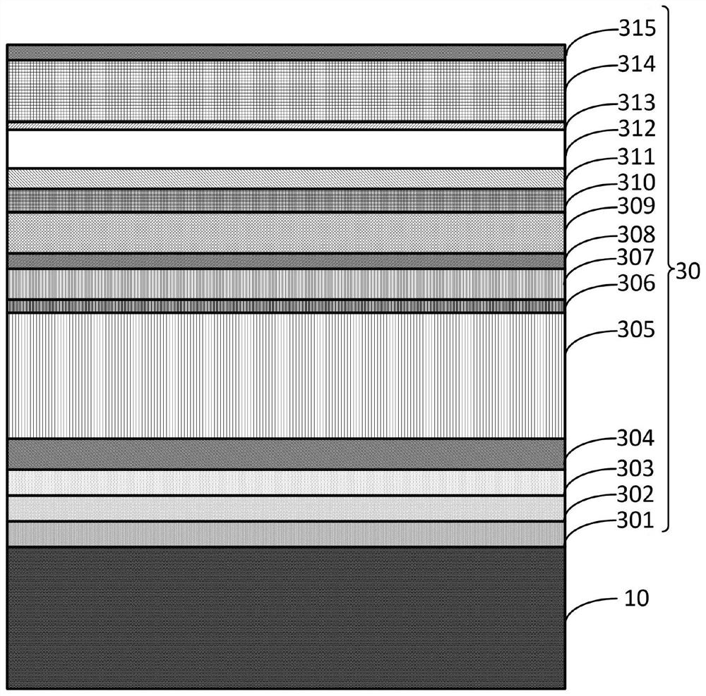
[0041] Before describing the embodiments according to the present invention, the following will be described in advance. First, in this specification, when only "GaInP" is indicated, the chemical composition ratio of the sum of Ga and In to P is 1:1, and an arbitrary compound in which the ratio of Ga and In is not constant. When only "AlGaInP" is indicated, the chemical composition ratio of the sum of Al, Ga, and In to P is 1:1, and any compound in which the ratio of Al, Ga, and In is not constant. In addition, when only "AlInP" is indicated, the chemical composition ratio of the sum of Al and In to P is 1:1, and an arbitrary compound in which the ratio of Al and In is not constant is indicated.

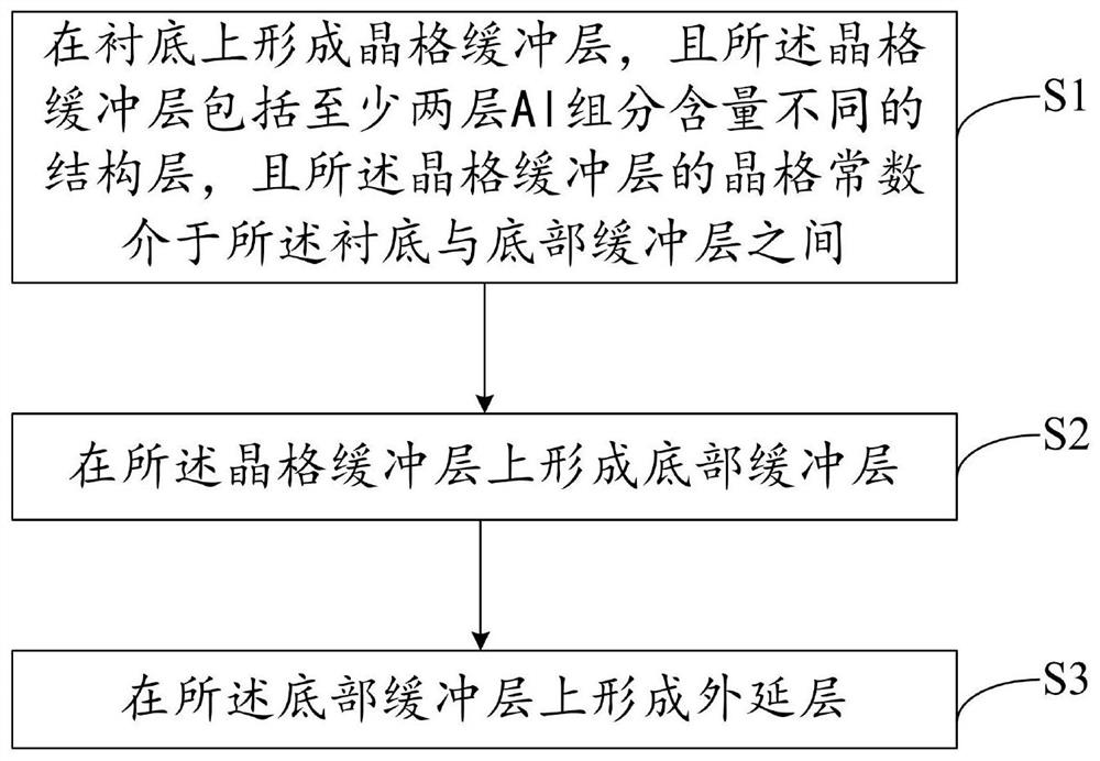
[0042] The epitaxial structure of the LED chip proposed by the present invention and the preparation method thereof will be further described in detail below in conjunction with the accompanying drawings and specific embodiments. The advantages and features of the present invention ...


PUM

PropertyMeasurementUnit
Thicknessaaaaaaaaaa
Thicknessaaaaaaaaaa

Abstract

The invention provides an LED chip epitaxial structure and a preparation method thereof. The LED chip epitaxial structure sequentially comprises a lattice buffer layer, a bottom buffer layer and an epitaxial layer from bottom to top, the lattice buffer layer, the bottom buffer layer and the epitaxial layer are formed on a substrate, and the lattice buffer layer comprises at least two structural layers with different Al component contents; and the lattice constant of the lattice buffer layer is between the substrate and the bottom buffer layer. The lattice buffer layer is formed between the substrate and the bottom buffer layer, the problems of thermal mismatch and lattice mismatch existing between the substrate and the epitaxial structure can be solved through the lattice buffer layer, impurities in the substrate can be prevented from entering the epitaxial structure, and the high-quality epitaxial structure is obtained.

Description

technical field [0001] The invention relates to the technical field of semiconductors, in particular to an LED chip epitaxial structure and a preparation method thereof. Background technique [0002] Light-emitting diodes (light-emitting diodes, LEDs) are expected to replace traditional incandescent lamps, fluorescent lamps and gas discharge lamps as a new generation of lighting sources due to their advantages of high efficiency, energy saving and environmental protection, long life, and small size, which has attracted a lot of attention in the fields of industry and scientific research. widespread attention. Since the first light-emitting diode was born in 1962, the performance of light-emitting diodes has been greatly improved in all aspects, and the application fields have become wider and wider. [0003] The Si substrate with mature production technology and low cost can effectively reduce the manufacturing cost of LED chips, and is also very suitable for preparing high...

Claims


Application Information

Patent Timeline
IPC IPC(8): H01L33/12H01L33/00
CPCH01L33/12H01L33/007
Inventor 赖玉财李森林毕京锋
Owner XIAMEN SILAN ADVANCED COMPOUND SEMICON CO LTD
Features
  • R&D
  • Intellectual Property
  • Life Sciences
  • Materials
  • Tech Scout
  • Unparalleled Data Quality
  • Higher Quality Content
  • 60% Fewer Hallucinations
Learn More