Eureka AIR delivers breakthrough ideas for toughest innovation challenges, trusted by R&D personnel around the world.

Preparation method of vertical gate semiconductor device

A semiconductor and vertical gate technology, applied in the field of vertical gate semiconductor device preparation, can solve the problems of easy leakage current, ineffective diffusion of doped ions, and decreased photosensitivity

Pending Publication Date: 2021-11-05
SHANGHAI HUALI MICROELECTRONICS CORP
View PDF4 Cites 2 Cited by
  • Summary
  • Abstract
  • Description
  • Claims
  • Application Information

AI Technical Summary

Problems solved by technology

[0002] In order to increase the number of pixels per unit area of ​​the image sensor, the pixel size of the image sensor is continuously reduced. The resulting problem is that the area of ​​the effective pixel area is greatly reduced, and the number of electrons in the photodiode is significantly reduced, resulting in a decrease in photosensitivity. The first way to decrease is to increase the ion implantation depth and concentration in the photodiode region
For the 2D planar gate structure, when the transfer gate is turned on, the electrons generated in the photodiode region are transferred to the floating diffusion region through the surface channel, and then read. This electron transfer method has a small path and low electron extraction efficiency, which is not conducive to fast read
[0003] The 3D vertical gate structure effectively solves the above-mentioned problems of slow electron transfer and low efficiency
For the 3D vertical gate, the existing technology still uses the 2D planar gate to grow polysilicon first, and then ion implantation, which prevents the dopant ions from effectively diffusing into the polysilicon deep in the vertical gate hole. The doping concentration is uneven, and there are impurities and lattice defects in the polysilicon layer, which can easily form a leakage current during photoelectron transfer, resulting in more white pixels when the image sensor is working

Method used


Image

  • Preparation method of vertical gate semiconductor device
  • Preparation method of vertical gate semiconductor device
  • Preparation method of vertical gate semiconductor device

Examples


preparation example Construction

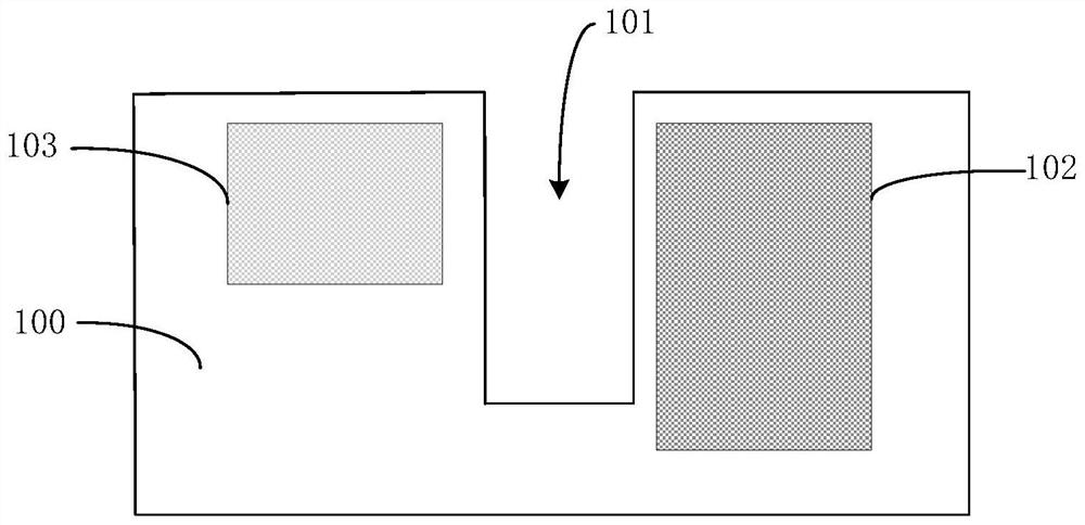
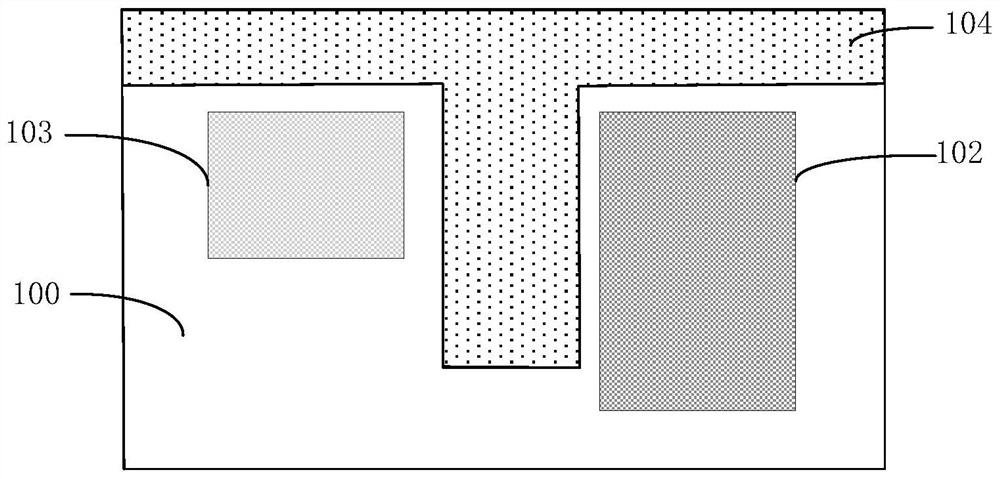
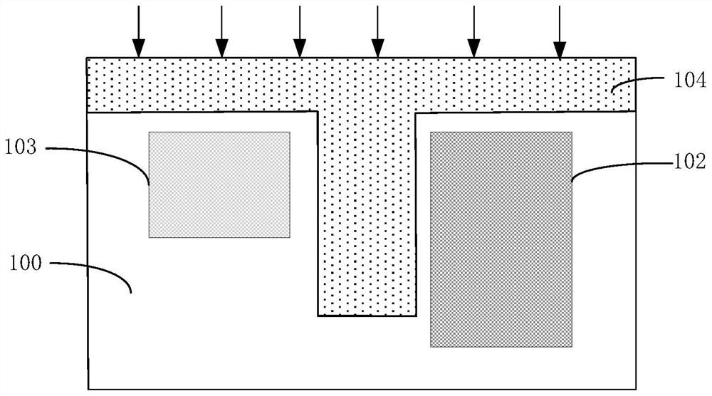
[0029] figure 2 A flow chart of a method for manufacturing a vertical gate semiconductor device provided in this embodiment, as shown in figure 2 As shown, this embodiment provides a method for fabricating a vertical gate semiconductor device, including:

[0030] Step S1: providing a substrate, a trench is formed in the substrate, and photodiode regions and floating diffusion regions respectively located on both sides of the trench;

[0031] Step S2: forming an amorphous silicon layer on the substrate, the amorphous silicon layer filling the trench, and injecting a doping gas to perform in-situ doping while forming the amorphous silicon layer;

[0032] Step S3: performing thermal annealing treatment on the amorphous silicon layer, so as to transform the amorphous silicon layer into a polysilicon layer.


PUM

PropertyMeasurementUnit
temperatureaaaaaaaaaa

Abstract

The invention provides a preparation method of a vertical semiconductor device. The method comprises the steps of: providing a substrate which is internally provided with a groove, as well as a photodiode region and a floating diffusion region which are located at the two sides of the groove respectively; forming an amorphous silicon layer on the substrate, filling the groove with the amorphous silicon layer, and introducing doping gas to perform in-situ doping while forming the amorphous silicon layer; and performing thermal annealing treatment on the amorphous silicon layer, and activating doped ions, so as to convert the amorphous silicon layer into a polycrystalline silicon layer. According to the preparation method of the vertical gate semiconductor device of the invention, the doped ions in the polycrystalline silicon are distributed more uniformly, impurities and lattice defects in the polycrystalline silicon are reduced, and the phenomena of leakage current and white pixel points in an image sensor are improved.

Description

technical field [0001] The invention relates to the field of semiconductor manufacturing, in particular to a method for preparing a vertical gate semiconductor device. Background technique [0002] In order to increase the number of pixels per unit area of ​​the image sensor, the pixel size of the image sensor is continuously reduced. The resulting problem is that the area of ​​the effective pixel area is greatly reduced, and the number of electrons in the photodiode is significantly reduced, resulting in a decrease in photosensitivity. The primary way to reduce this is to increase the ion implantation depth and concentration in the photodiode region. For the 2D planar gate structure, when the transfer gate is turned on, the electrons generated in the photodiode region are transferred to the floating diffusion region through the surface channel, and then read. This electron transfer method has a small path and low electron extraction efficiency, which is not conducive to fas...

Claims


Application Information

Patent Timeline
Patent Type & Authority Applications(China)
IPC IPC(8): H01L27/146H01L21/28H01L29/423
CPCH01L27/14689H01L27/14614H01L29/4236H01L29/401
Inventor 陈彩云张磊顾珍董立群王奇伟陈昊瑜
Owner SHANGHAI HUALI MICROELECTRONICS CORP
Why Eureka
Eureka Blog
Learn More