Method for preparing 3D printing resistor and adjusting resistance value

A 3D printing and adjustment method technology, which is applied in the direction of resistor manufacturing, resistors, and fine-tuning resistors, etc., can solve the problems of uncontrollable resistor thickness differences, inconsistent resistors, and multiple pastes, so as to reduce the risk of falling off and reduce materials. Wasteful, easy-to-integrate effects

Active Publication Date: 2021-11-09
西安瑞特三维科技有限公司
View PDF6 Cites 1 Cited by
  • Summary
  • Abstract
  • Description
  • Claims
  • Application Information

AI Technical Summary

Problems solved by technology

[0004]Using screen printing resistor paste to make resistors, the thickness of the overall carbon paste tends to be consistent, and it is impossible to control the difference in resistor thickness
It is necessary to customize a special screen or steel screen, and more slurry will be wasted during the screen printing process
After printing, due to the flow and spread of the slurry, the resistance is inconsistent. Usually, the laser resistance trimmer is used to trim the resistance, and the laser resistance trimming method is only applicable to the case where the resistance value is lower than the target resistance value. trim

Method used


Image

  • Method for preparing 3D printing resistor and adjusting resistance value
  • Method for preparing 3D printing resistor and adjusting resistance value
  • Method for preparing 3D printing resistor and adjusting resistance value

Examples


Embodiment example 1

[0038] The target resistance value is: 160Ω±10%, the electrode spacing is: 0.3mm, the base material is PET; the design square resistance size is: 1.6mm×1.6mm, the thickness: subject to the actual printing thickness (20~50μm), the printed resistance The slurry is: carbon slurry (Xi'an Ruite 3D Technology Co., Ltd.), viscosity: (4~5)×10 4 Cp, square resistance: 1KΩ / □, curing temperature 160℃@0.5h. Equipment: Dual micro-pen direct writing 3D printer (Model: JD200Pro, Xi'an Ruite 3D Technology Co., Ltd.)

[0039] The printing parameters are: needle diameter: 0.24mm, printing air pressure: 0.38Mpa, layer height 0.1mm, printing speed 100mm / min

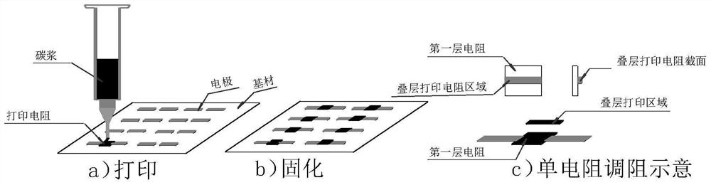
[0040] Printing resistance result: The resistance value actually tested by a multimeter is 250Ω±10%, the specific data is shown in Table 1, and the appearance is shown in Figure 4 a).

[0041] The design size of the resistance adjustment pattern: 1.6mm×0.4mm, the height from the substrate layer: 0.15mm, other printing parameters and the ...

Embodiment example 2

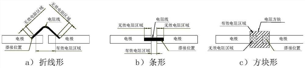
[0044] Different resistance between fixed electrodes can be achieved by designing different graphics, such as designed bar, square, round, S-shaped, etc. The electrode spacing is 4mm, the electrode size is 2*2mm, the selected resistance slurry is graphene slurry, the viscosity is 3~6*10 4 , the square resistance is 25Ω@20μm, the curing temperature is: 150℃@30min, and the base material is PI film. Equipment: Dual micro-pen direct writing 3D printer (Model: JD200Pro, Xi'an Ruite 3D Technology Co., Ltd.)

[0045] Printing parameters: the diameter of the printing needle is 0.16mm, the air pressure is 0.2Mpa, the layer height is 0.1mm, and the printing speed is 400mm / min.

[0046] The printing resistance and graphics of different design graphics are shown in Table 2.

[0047] Table 1 Printed resistance and resistance value change after stacking

[0048]

[0049] Table 2 Print the resistors of different design graphics

[0050]

[0051] The present invention uses an oven, ...


PUM


Abstract

The invention discloses a method for preparing a 3D printing resistor and adjusting the resistance value. The method comprises the following steps of: firstly, preliminarily designing the graphic size of the printed resistor according to information including the distance between electrodes, the space size and the required target resistance value, secondly, calculating the sheet resistance value or the resistivity of a material needing to be printed, and screening printed resistor slurry or printing ink; generating a printing path file of the resistor; fixing the base material on a printer base table, adjusting printing parameters, and completing resistor printing; after the printed resistor is cured and sintered, testing the resistor, comparing with a target resistance value, and if the target resistance value design is met, finishing printing; and if not, adjusting the resistance value by adopting an optimized design pattern size or printing parameters, or adjusting the resistance value on the basis of the printed and cured resistor. According to the invention, screen plate manufacturing and material waste in a traditional silk-screen printing process can be avoided, in addition, the resistor pattern and the resistor thickness can be flexibly adjusted, and the problem that the thickness is difficult to accurately adjust in silk-screen printing is avoided.

Description

technical field [0001] The invention belongs to the field of processing and manufacturing resistance elements, and in particular relates to a method for preparing and adjusting resistance value of 3D printed resistance. Background technique [0002] Resistors are one of the commonly used components in electronic equipment. Usually, resistors are deposited on an insulating substrate by using screen-printed resistive materials, and sintered to form thick film chip resistors; metal chip resistors are evaporated and sputtered in vacuum. Processes such as sputtering resistive materials on insulating substrates. After being packaged, it is fixed on the electronic circuit board in the form of welding, which usually requires professional equipment for automatic placement and reflow soldering. The chip resistors on the flexible film are small in size, and in the subsequent bending or secondary processing of the film, the chip resistors are easily deformed by bending or scratched by ...

Claims


Application Information

Patent Timeline
Patent Type & Authority Applications(China)
IPC IPC(8): H01C17/065H01C17/22
CPCH01C17/065H01C17/22
Inventor 李超尹恩怀冯瑶瑶鱼春龙袁学礼
Owner 西安瑞特三维科技有限公司
Why Eureka
Try Eureka