Optical arrangement and lithography apparatus
A technology of optical devices and lithography equipment, applied in the field of optical devices and lithography equipment, can solve the problems of increasing capacitive interaction and disadvantages
- Summary
- Abstract
- Description
- Claims
- Application Information
AI Technical Summary
Problems solved by technology
Method used
Image

Examples
Embodiment Construction
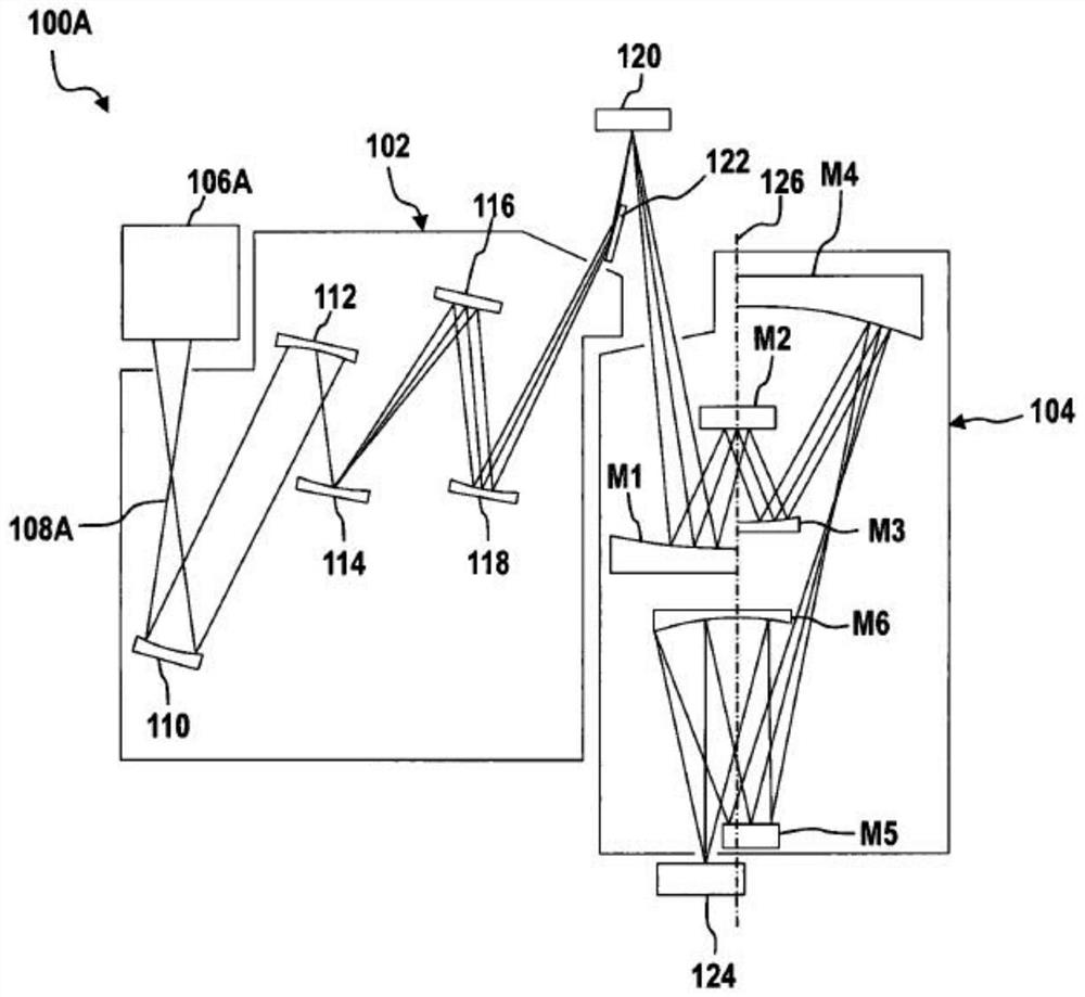
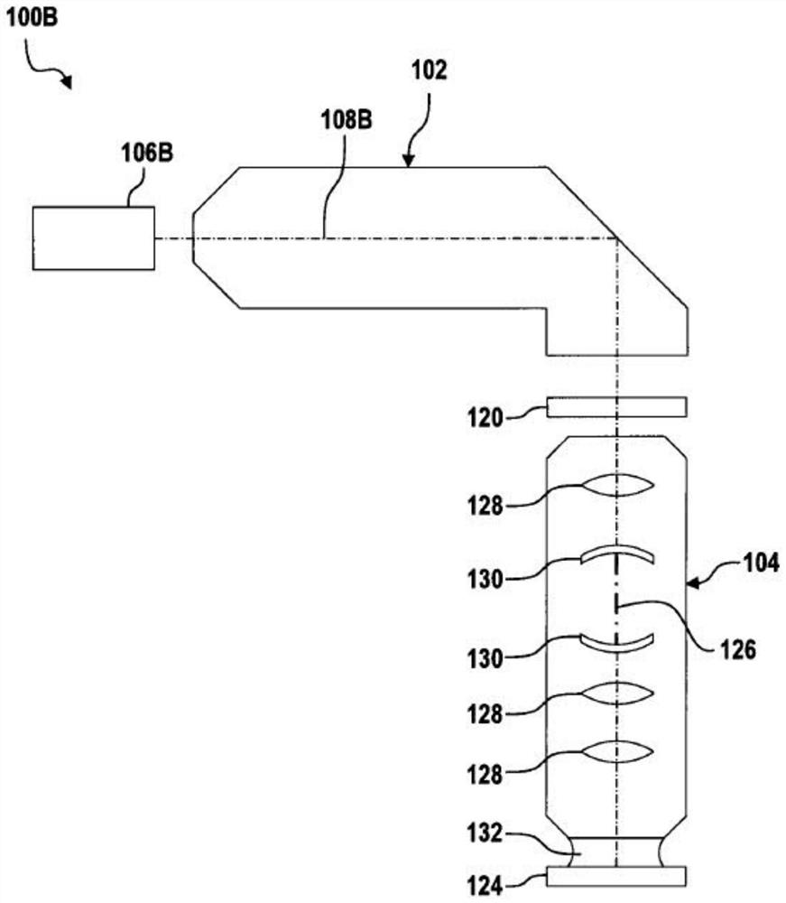
[0082] Figure 1AA schematic diagram of an EUV lithographic apparatus 100A including a beam shaping and illumination system 102 and a projection system 104 is shown. In this case, EUV stands for "extreme ultraviolet," meaning the wavelengths of light at work are between 0.1 nanometers and 30 nanometers. The beam shaping and illumination system 102 and the projection system 104 are respectively arranged in vacuum enclosures (not shown), wherein each vacuum enclosure is evacuated by means of an evacuation device (not shown). The vacuum enclosure is surrounded by a machine room (not shown) in which drive means for mechanically moving or setting the optical elements are provided. In addition, electrical controllers and the like can also be set in the machine room.
[0083] The EUV lithographic apparatus 100A has a EUV radiation source 106A. A plasma source (or synchrotron) emitting radiation 108A in the EUV range (extreme ultraviolet range), that is to say for example in the wav...
PUM
| Property | Measurement | Unit |
|---|---|---|
| size | aaaaa | aaaaa |
| wavelength | aaaaa | aaaaa |
Abstract
Description
Claims
Application Information