Laser detection unit circuit, laser detection integrated circuit, and semiconductor chip

A technology of laser detection and unit circuit, which is applied in the field of semiconductors, can solve the problems of low security and too large area of ​​PNP transistors, etc., and achieve the effect of improving security, avoiding the possibility of being attacked, and reducing the possibility

Pending Publication Date: 2021-11-12
CHINA MOBILE M2M +1
View PDF0 Cites 0 Cited by
  • Summary
  • Abstract
  • Description
  • Claims
  • Application Information

AI Technical Summary

Problems solved by technology

[0005] The embodiment of the present invention provides a laser detection unit circuit, a laser detection integrated circuit and a semiconductor chip to solve the problem of low safety of the existing laser detection circuit due to the excessive area of ​​the PNP transistor

Method used


Image

  • Laser detection unit circuit, laser detection integrated circuit, and semiconductor chip
  • Laser detection unit circuit, laser detection integrated circuit, and semiconductor chip
  • Laser detection unit circuit, laser detection integrated circuit, and semiconductor chip

Examples


Embodiment Construction

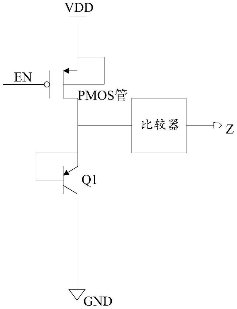
[0018] It can be seen from the background art that laser detection circuits composed of PNP transistors are not suitable as light detectors for semiconductor chips, because they are not suitable for automatic placement by automatic layout tools. Due to the large area of ​​the PNP transistor, the physical boundary is obvious, and it is larger than the general standard unit, it is easy for the attacker to find, locate and avoid it during the actual attack process, so that the laser detection circuit does not play its actual detection role.

[0019] At the same time, due to the large area of ​​the PNP transistor, the area of ​​the laser detection circuit is relatively large, which is easy to be discovered and attacked by an attacker, resulting in low security. For example, an attacker attacks the enable switch in the laser detection circuit, so that the detection function of the laser detection circuit is lost.

[0020] Moreover, the PNP triode is an analog device, which must be ...


PUM


Abstract

The invention provides a laser detection unit circuit, a laser detection integrated circuit and a semiconductor chip. The laser detection unit circuit includes a photosensitive device, a path switching device and an inverting device, and the photosensitive device is an MOS tube; the first end of the path switching device is connected with a first voltage end, the second end of the path switching device is connected with the third end of the path switching device, the third end of the path switching device is connected with the first end of the photosensitive device, the second end of the photosensitive device is connected with the third end of the photosensitive device, and the third end of the photosensitive device is connected with a second voltage end; the input end of the inverting device is connected with the first end of the photosensitive device; under the condition that the photosensitive device senses laser irradiation, the conduction state of the first end of the photosensitive device and the conduction state of the third end of the photosensitive device are changed, and high-low conversion occurs to the voltage of the first end of the photosensitive device, so that the inverting device outputs a first alarm signal. According to the embodiment of the invention, the safety of the laser detection unit circuit can be improved.

Description

technical field [0001] The embodiments of the present invention relate to the technical field of semiconductors, and in particular to a laser detection unit circuit, a laser detection integrated circuit and a semiconductor chip. Background technique [0002] In order to prevent the semiconductor chip from being attacked by the laser, it is necessary to arrange a detection circuit in the semiconductor chip to realize the detection of the semiconductor chip being attacked by the laser. [0003] At present, photosensitive devices are usually integrated in semiconductor chips, see figure 1 , figure 1 It is a schematic structural diagram of a detection circuit used in the prior art to detect that a semiconductor chip is attacked by a laser. Such as figure 1 As shown, Q1 is a transistor, which is a triode (referred to as a PNP triode) composed of two P-type semiconductors sandwiching an N-type semiconductor, and belongs to a photosensitive device. In the detection circuit, whe...

Claims


Application Information

Patent Timeline
IPC IPC(8): G01R31/265H01L27/146
CPCG01R31/2656H01L27/14612
Inventor 朱磊戴山彪肖青孙东昱张亚双
Owner CHINA MOBILE M2M
Why Eureka
Try Eureka