Semiconductor structure and forming method of semiconductor structure

A semiconductor, fork-shaped structure technology, applied in the fields of semiconductor devices, semiconductor/solid-state device manufacturing, nanotechnology for information processing, etc. The effect of enhancing the isolation effect

Pending Publication Date: 2021-11-19
SEMICON MFG INT (SHANGHAI) CORP +1
View PDF0 Cites 1 Cited by
  • Summary
  • Abstract
  • Description
  • Claims
  • Application Information

AI Technical Summary

Problems solved by technology

[0004] However, the performance of fork-shaped nanosheets still needs to be improved

Method used


Image

  • Semiconductor structure and forming method of semiconductor structure
  • Semiconductor structure and forming method of semiconductor structure
  • Semiconductor structure and forming method of semiconductor structure

Examples


Embodiment Construction

[0039] As mentioned in the background art, the performance of the existing fork-shaped nanosheets still needs to be improved. Now analyze and illustrate in conjunction with specific embodiment.

[0040] It should be noted that the "surface" in this specification is used to describe the relative positional relationship in space, and is not limited to direct contact.

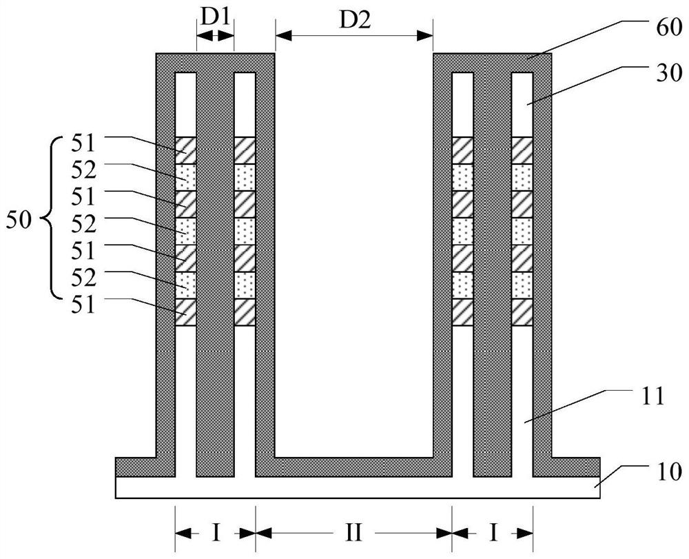
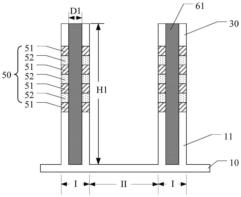
[0041] Figure 1 to Figure 3 It is a schematic cross-sectional structure diagram of a semiconductor structure.

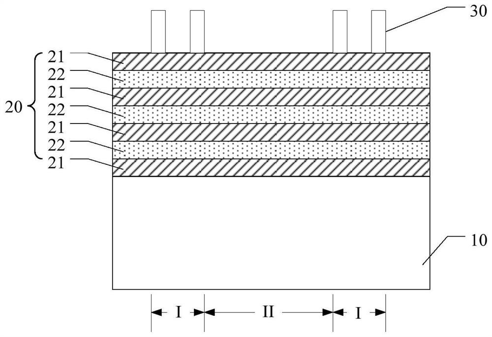
[0042] Please refer to figure 1 , provide a substrate 10, the substrate 10 includes several first regions I, and the second region II between adjacent first regions I; form a composite nanosheet material layer 20 on the substrate 10; Two separate mask structures 30 are formed on the surface of the composite nanosheet material layer 20 in the first region I.

[0043] The composite nanosheet material layer 20 includes: several sacrificial material layers 21 , and nanosheet material layers 22 located b...


PUM


Abstract

The invention discloses a semiconductor structure and a forming method of the semiconductor structure. The method comprises the following steps that a substrate is provided; a plurality of separated fork-shaped structures are formed on the substrate, a first opening is formed between every two adjacent fork-shaped structures, each fork-shaped structure comprises a fin part structure located on the surface of the substrate, a composite nanosheet structure located on the fin part structure, and a second opening penetrating through the composite nanosheet structure, the second opening extends into the fin part structure, and the depth of the second opening is lower than that of the first opening; and an isolation structure is formed in the second openings. Therefore, the performance of the semiconductor structure is improved.

Description

technical field [0001] The invention relates to the field of semiconductor manufacturing, in particular to a semiconductor structure and a method for forming the semiconductor structure. Background technique [0002] The FinFET transistor architecture is the workhorse of today's semiconductor industry. However, as the device continues to shrink, when the channel length is small to a certain value, the fin field effect transistor structure cannot provide sufficient electrostatic control and sufficient driving current. Therefore, a nanosheet (Nanosheet) structure is introduced. Compared with FinFETs, the properties of nanosheets provide excellent channel control capabilities. At the same time, the excellent distribution of the channels in three dimensions enables the optimization of the effective driving current per unit area. [0003] As the journey to smaller track heights continues, further reductions in cell height will require smaller pitches between NMOS and PMOS devic...

Claims


Application Information

Patent Timeline
Patent Type & Authority Applications(China)
IPC IPC(8): H01L21/336H01L29/78B82Y40/00B82Y10/00
CPCH01L29/66803H01L29/785B82Y40/00B82Y10/00H01L29/0673H01L29/775
Inventor 郑二虎
Owner SEMICON MFG INT (SHANGHAI) CORP
Why Eureka
Try Eureka