Flat coupling ridge waveguide semiconductor laser

A ridge waveguide and semiconductor technology, applied in the field of semiconductor laser devices, can solve the problems of high cavity surface power density, optical cavity surface catastrophe, narrow mode field area, etc., and achieve the goal of improving laser output power, good beam quality, and reducing power density Effect

Pending Publication Date: 2021-11-26
INST OF APPLIED ELECTRONICS CHINA ACAD OF ENG PHYSICS
View PDF5 Cites 0 Cited by
  • Summary
  • Abstract
  • Description
  • Claims
  • Application Information

AI Technical Summary

Problems solved by technology

Due to the small cross-sectional area of ​​the narrow ridge waveguide, the supported mode field area is narrow, resulting in high cavity surface power

Method used


Image

  • Flat coupling ridge waveguide semiconductor laser

Examples


Example Embodiment

[0028] Example 1

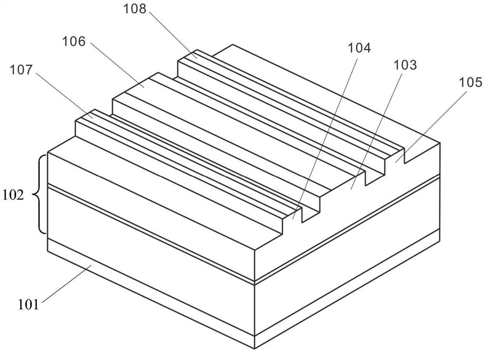
[0029] like figure 1 As shown, in this embodiment, a slab-coupled ridge waveguide semiconductor laser is specifically provided, aiming to further increase the total laser output power under the premise of maintaining better beam quality through optimization and improvement of the semiconductor laser. In this embodiment, a 976nm semiconductor laser is used, and the 976nm semiconductor laser mainly includes: a common electrode 101 and an epitaxial layer 102 that are stacked and arranged in sequence.

[0030] Three ridge waveguides are provided on the top of the epitaxial layer 102, respectively the first ridge waveguide 103, the second ridge waveguide 104 and the third ridge waveguide 105, wherein the first ridge waveguide 103 is a wide ridge waveguide and the second ridge waveguide 104 and The third ridge waveguide 105 is a narrow ridge waveguide, and the width of the narrow ridge waveguide is smaller than the width of the wide ridge waveguide. In this embo...

Example Embodiment

[0035] Example 2

[0036]In this embodiment, a slab-coupled ridge waveguide semiconductor laser is specifically provided, aiming to further increase the total output power of the laser on the premise of maintaining better beam quality through optimization and improvement of the semiconductor laser. In Embodiment 1 On the basis, the design of the semiconductor laser is as follows:

[0037] Three ridge waveguides are provided on the top of the epitaxial layer 102, respectively the first ridge waveguide 103, the second ridge waveguide 104 and the third ridge waveguide 105, wherein the first ridge waveguide 103 is a wide ridge waveguide and the second ridge waveguide 104 And the third ridge waveguide 105 is a narrow ridge waveguide, the width of the narrow ridge waveguide is smaller than the width of the wide ridge waveguide. In this embodiment, the second ridge waveguide 104 and the third ridge waveguide 105 are located on both sides of the first ridge waveguide 103 and distribu...


PUM

PropertyMeasurementUnit
Widthaaaaaaaaaa
Widthaaaaaaaaaa

Abstract

The invention discloses a flat coupling ridge waveguide semiconductor laser and belongs to the technical field of semiconductor laser devices. The flat coupling ridge waveguide semiconductor laser comprises an epitaxial layer; the top of the epitaxial layer is provided with a wide ridge waveguide and narrow ridge waveguides respectively located at two sides of the wide ridge waveguide; the transverse electric field mode of the wide ridge waveguide is limited through each narrow ridge waveguide, and the width of each narrow ridge waveguide is smaller than that of the wide ridge waveguide; and forward bias voltage is applied to the wide ridge waveguide, and reverse bias voltage is applied to each narrow ridge waveguide, so that the purposes of improving the output power of a single laser and keeping better light beam quality can be achieved.

Description

technical field [0001] The invention belongs to the technical field of semiconductor laser devices, and in particular relates to a flat plate coupled ridge waveguide semiconductor laser. Background technique [0002] Slab waveguide semiconductor lasers have the advantages of simple structure, high power, and low cost, and are widely used in laser medical treatment, free space optical communication, pump source, phased array radar, and advanced material processing. Among them, the slab waveguide semiconductor laser near the wavelength of 976nm is mainly used for the pumping of the ytterbium-doped fiber laser, which can obtain higher light-to-light conversion efficiency. [0003] Although the current slab waveguide semiconductor lasers have high output power, they have multi-mode lasing, and the beam quality of the output laser is poor, which limits the application of slab waveguide semiconductor lasers. The main method to improve the beam quality is in slab waveguide semicond...

Claims


Application Information

Patent Timeline
IPC IPC(8): H01S5/22H01S5/065
CPCH01S5/22H01S5/2202H01S5/0653
Inventor 贺钰雯周坤杜维川李弋何林安高松信唐淳
Owner INST OF APPLIED ELECTRONICS CHINA ACAD OF ENG PHYSICS
Why Eureka
Try Eureka