A production equipment and method for forming a conductive layer on the solder-resisting surface of a circuit board

A technology for production equipment and conductive layers, applied in the directions of printed circuits, printed circuit manufacturing, and manufacturing of printed circuit precursors. , the effect of reducing labor intensity and improving molding efficiency

Active Publication Date: 2022-01-25
四川英创力电子科技股份有限公司
View PDF9 Cites 0 Cited by
  • Summary
  • Abstract
  • Description
  • Claims
  • Application Information

AI Technical Summary

Problems solved by technology

[0003] However, although the production process used in the workshop can form the conductive layer, the following technical defects are still found in the actual production process: 1. It is necessary to manually pre-assemble and position four enclosures around the substrate, and manual positioning exists. The problem of inaccurate positioning, that is, when there is a gap between two adjacent panels, the filled copper paste will flow out of the gap, which will cause the thickness of the conductive layer on each semi-finished circuit board to be inconsistent, thereby greatly reducing the Molding quality of the conductive layer
2. The viscosity of the copper paste is high, and workers need to spend a lot of time and a lot of effort to push the copper paste to flow, resulting in a long time for scraping the copper paste, resulting in a longer forming time for the conductive layer, which greatly reduces the electrical conductivity. Layer Forming Efficiency
3. The method of baking the conductive layer in the oven is single, that is, only the outer surface of the conductive layer can be baked, resulting in uneven heating of the conductive layer and deformation of the surface, which further reduces the molding quality of the conductive layer

Method used


Image

  • A production equipment and method for forming a conductive layer on the solder-resisting surface of a circuit board
  • A production equipment and method for forming a conductive layer on the solder-resisting surface of a circuit board
  • A production equipment and method for forming a conductive layer on the solder-resisting surface of a circuit board

Examples


Embodiment Construction

[0033] The present invention will be further described below in conjunction with accompanying drawing, protection scope of the present invention is not limited to the following:

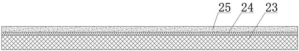
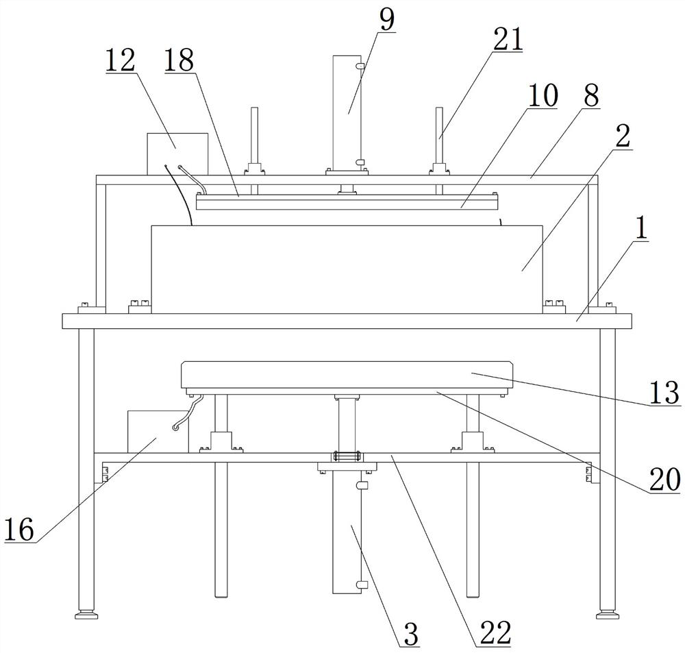
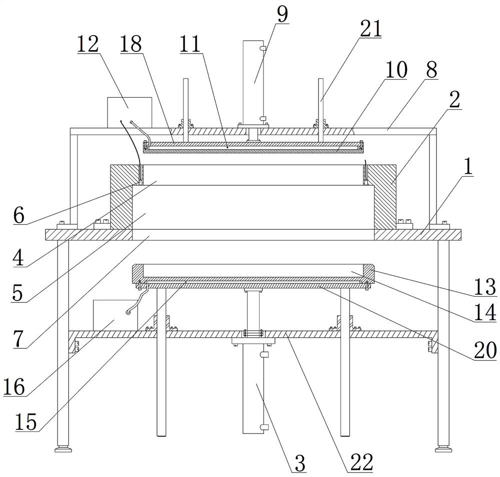
[0034] Such as Figure 2~7 As shown, a production equipment for forming a conductive layer on the solder-resisting surface of a circuit board, it includes a workbench 1, a base 2 fixed on the workbench 1, and a lifting cylinder 3 arranged below the workbench 1. The top surface of the base 2 is provided with an upper through groove 4 and a positioning groove 5 sequentially along its axial direction, and the outer contour of the lower through groove 7 is flush with the positioning groove 5. Shoulder, a plurality of heating blocks 6 are arranged in the top end of the base 2 and along the circumferential direction of the upper through groove 4, and a lower through groove 7 communicating with the positioning groove 5 is provided on the table surface of the workbench 1, and the table surface of the workben...


PUM


Abstract

The invention discloses a production equipment and method for forming a conductive layer on the solder-resisting surface of a circuit board, which comprises a workbench (1), a base (2) fixed on the workbench (1), and a (1) The lifting cylinder (3) below, the top surface of the base (2) is provided with an upper through groove (4) and a positioning groove (5) in sequence along its axial direction, and the positioning groove (5) is connected with the upper through A shoulder is formed between the grooves (4), and a lower through groove (7) connected to the positioning groove (5) is opened on the table surface of the workbench (1), and an extrusion cylinder ( 9), the piston rod of the extrusion cylinder (9) is set through the beam, and the extension end is provided with a pressure plate (10). The beneficial effects of the invention are: compact structure, reducing labor intensity of workers, ensuring uniform thickness of the conductive layer, improving the forming quality of the conducting layer, and improving the forming efficiency of the conducting layer.

Description

technical field [0001] The invention relates to the technical field of forming a conductive layer on a substrate, in particular to a production equipment and method for forming a conductive layer on a solder-resisting surface of a circuit board. Background technique [0002] With the continuous development of communication technology, different types of communication equipment emerge as the times require, and circuit boards that control the operation of communication equipment must be installed in various communication equipment, so the production and processing of circuit boards is becoming more and more important. The process requires adding a conductive layer on the top surface of the substrate with a solder mask layer to obtain a semi-finished circuit board, and then transport the semi-finished circuit board to the post-production process to finally produce a product circuit board. Among them, the structure of the semi-finished circuit board is as follows: figure 1 As s...

Claims


Application Information

Patent Timeline
Patent Type & Authority Patents(China)
IPC IPC(8): H05K3/02
CPCH05K3/022
Inventor 胡志强艾克华牟玉贵杨海军邓岚张仁军
Owner 四川英创力电子科技股份有限公司
Why Eureka
Try Eureka