Shield gate MOSFET device, chip and terminal equipment

A technology for shielding gates and devices, applied in semiconductor devices, electrical components, circuits, etc., can solve problems affecting device frequency characteristics and switching loss, etc.

Pending Publication Date: 2021-12-03
VANGUARD SEMICON CORP
View PDF8 Cites 0 Cited by
  • Summary
  • Abstract
  • Description
  • Claims
  • Application Information

AI Technical Summary

Problems solved by technology

[0004] In view of this, this application provides a shielded gate MOSFET device, chip and terminal equipment to solve the technical problem that the gate-source capacitance of the shielded gate MOSFET device increases and affects the frequency characteristics and switching loss of the device

Method used


Image

  • Shield gate MOSFET device, chip and terminal equipment
  • Shield gate MOSFET device, chip and terminal equipment
  • Shield gate MOSFET device, chip and terminal equipment

Examples


Embodiment Construction

[0030] The technical solutions in the embodiments of the present application will be clearly and completely described below in conjunction with the accompanying drawings. Apparently, the described embodiments are only some of the embodiments of the present application, not all of them. Based on the embodiments in this application, all other embodiments obtained by those skilled in the art without making creative efforts belong to the scope of protection of this application. In the case of no conflict, the following embodiments and technical features thereof can be combined with each other.

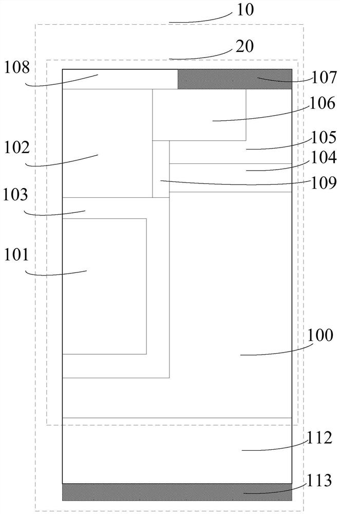
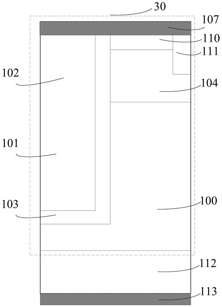
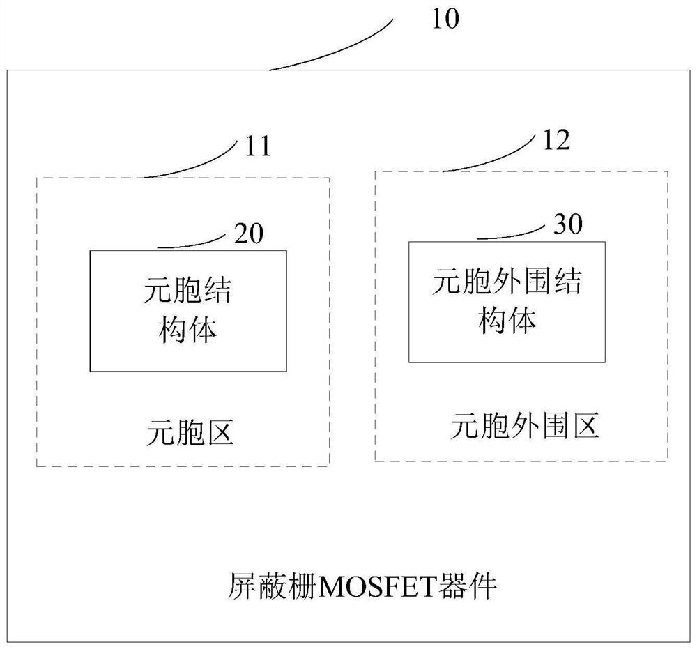
[0031] Such as figure 1 As shown, a shielded gate MOSFET device 10 is provided, including a cellular structure 20, the cellular structure 20 includes a first conductivity type drift region 100, and a first upper surface of the first conductivity type drift region 100 is provided with a shielded gate 101 .

[0032] A control grid 102 is arranged above the shielding grid 101, and a first i...


PUM


Abstract

The invention relates to a shield gate MOSFET device, a chip and an equipment terminal. A cell structure body in the shield gate MOSFET device comprises a first conduction type drift region, a shield gate is arranged on the first upper surface of the first conduction type drift region, a control gate is arranged above the shield gate, a first isolation layer is arranged between the first conduction type drift region and the shield gate, a second conduction type base region is arranged on the second upper surface of the first conduction type drift region, a first conduction type source region is arranged above the second conduction type base region, a third upper surface, close to the control gate, in the first conductive type source region is provided with a second isolation layer, a part of the upper surface of the second isolation layer and a fourth upper surface, away from the control gate, in the first conductive type source region are provided with a source electrode metal layer. and the thickness difference of the drift layer in the areas of the second upper surface and the first upper surface is greater than the thickness sum of the shield grid and the first isolation layer. According to the shield gate MOSFET device, the gate source capacitance is reduced.

Description

technical field [0001] The present application relates to the technical field, in particular to a shielded gate MOSFET device, chip and terminal equipment. Background technique [0002] Shielded gate MOSFET devices have the advantages of low conduction loss, low gate charge, fast switching speed, low device heat generation and high energy efficiency. The products can be widely used in personal computers, notebook computers, mobile phones, lighting products, televisions (LCD or plasma Power supplies or adapters for high-end consumer electronics such as televisions) and game consoles. [0003] Among them, the shielded gate MOSFET device introduces a shielded gate under the control gate, which avoids direct contact between the control gate and the drift region, thus greatly reducing the gate-to-drain capacitance. However, since the shielding gate is connected to the gate potential, a new gate-source capacitance will be generated between the control gate and the shielding gate,...

Claims


Application Information

Patent Timeline
Patent Type & Authority Applications(China)
IPC IPC(8): H01L29/06H01L29/78
CPCH01L29/0615H01L29/7831
Inventor 李伟聪姜春亮林泳浩雷秀芳
Owner VANGUARD SEMICON CORP
Why Eureka
Try Eureka