Super junction device

A super-junction device and super-junction technology, applied in the field of semiconductor integrated circuits, can solve the problems of no test instability, deterioration of matching state, easy under-matching, etc., to improve test instability, increase breakdown voltage, process good compatibility

Active Publication Date: 2021-12-10
SHANGHAI HUAHONG GRACE SEMICON MFG CORP
View PDF14 Cites 2 Cited by
  • Summary
  • Abstract
  • Description
  • Claims
  • Application Information

AI Technical Summary

Problems solved by technology

[0025] 1. At the position indicated by the dotted line box 105a, since both the left groove and the right groove top position will help depletion, this position is easy to over-match
[0026] 2. At the position indicated by the dotted line box 105b, due to the smooth effect of the groove head and the competition at the position indicated by the dotted line box 105a, the position indicated by the dotted line box 105b is prone to under-matching
[0027] 3. For any direction change at the dotted box 105a and 105b, process fluctuation or active design, size expansion or reduction, will lead to deterioration of the matching state of one of the two positions of the dotted box 105a and 105b
[0036] like Figure 4B Shown is the relationship curve 403 between the drain voltage and time during the breakdown voltage test of the first existing super-junction device. The surface of the curve 403 is relatively flat, and there is no test instability problem

Method used


Image

  • Super junction device
  • Super junction device
  • Super junction device

Examples


Embodiment Construction

[0083] The present invention is obtained on the basis of an in-depth analysis of the cause of the non-steady-state problem of the existing second super-junction device, that is, the unsteady state of the test of the all-straight strip design, and the reasons are as follows:

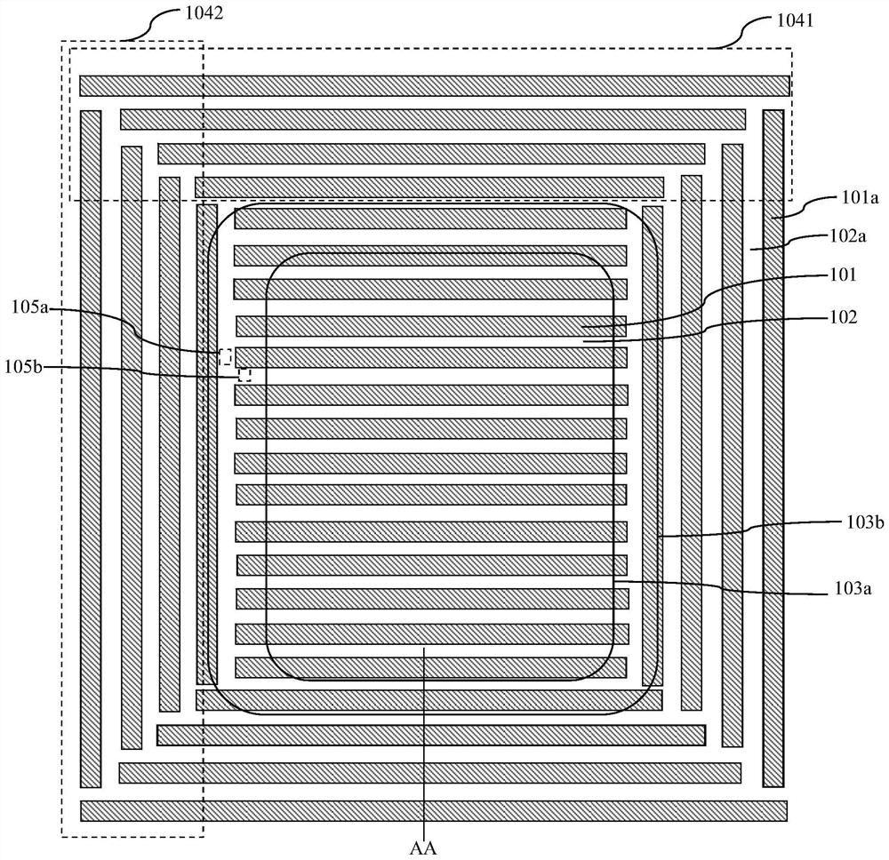
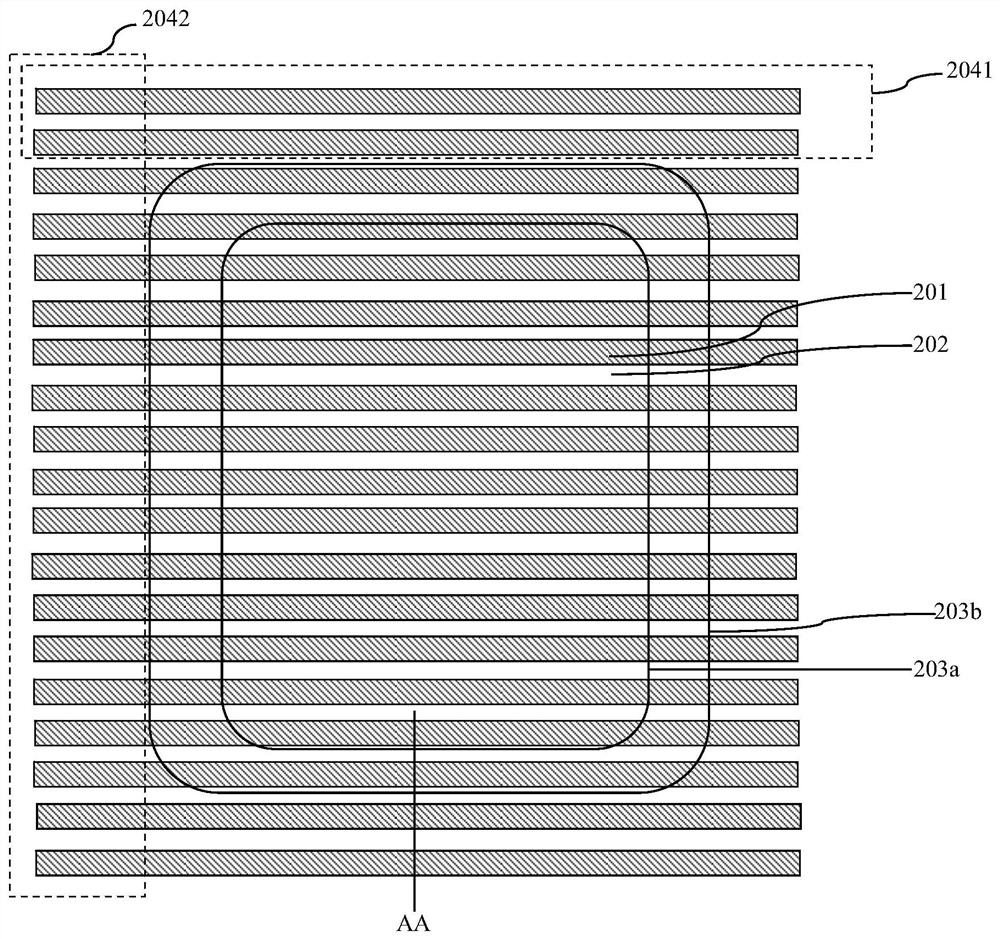
[0084] Compare Figure 2B and Figure 1B It can be seen from the structure shown that the first terminal area of ​​the straight bar design is similar to the structure of the terminal areas in two directions of the back-shaped design, that is, the first terminal area and the second terminal area. The follow-up mainly analyzes the first terminal area of ​​the straight bar design Second terminal area.

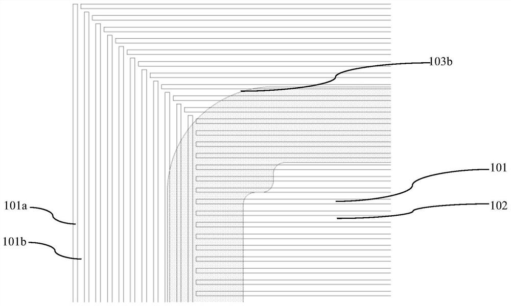
[0085] For the first terminal area: the cross-sectional structure of the first terminal area is as follows Figure 5 As shown, each P-type column 3 is floating, and as the drain voltage rises, the depletion region gradually expands from the inside to the outside, that is, along the Figure 5 The direction of...


PUM


Abstract

The invention discloses a super junction device. A charge flow region comprises a first super junction structure formed by alternately arranging first P-type columns and first N-type columns. In the width direction of the first P-type columns, the first P-type columns and the first N-type columns continue to be alternately arranged and enter the first terminal area. In the length direction of the first P-type columns, the first P-type columns and the first N-type columns of the charge flow region directly extend into a partial region, namely a straight strip-shaped region, of the second terminal region, and a region shaped like a Chinese character 'hui' is arranged on the outer side of the straight strip-shaped region. And the width of the straight strip-shaped region is set according to the widening width of the depletion region in the second terminal region when the super junction device is withstand voltage. And a second super junction structure formed by alternately arranging second P-type columns and second N-type columns is arranged in the rectangular-ambulatory-plane region. According to the invention, the advantages of the full-straight-strip-shaped super junction structure and the homocentric-square-shaped super junction structure can be compatible and the defects of the two super junction structures can be overcome, so that the breakdown voltage of the device can be improved and the problem of unstable test of the device can be solved.

Description

technical field [0001] The invention relates to a semiconductor integrated circuit, in particular to a super junction device. Background technique [0002] Super junction products are a device structure such as a MOSFET structure that uses PN charge balance to reduce the surface electric field (Resurf) technology in the body to increase the reverse breakdown voltage (BV) of the device while maintaining a small on-resistance. The PN-spaced pillar (Pillar) structure, that is, the structure of alternately arranged P-type pillars and N-type pillars, is the biggest feature of the super junction. At present, there are mainly two methods for making a pillar structure with PN intervals, one is obtained by multiple epitaxy (EPI) and ion implantation, and the other is made by deep trench etching and EPI filling. [0003] The key to the design of super-junction terminals is the layout structure design of the column. There are two typical designs, one is a zigzag design, and the other ...

Claims


Application Information

Patent Timeline
Patent Type & Authority Applications(China)
IPC IPC(8): H01L29/06H01L29/78H01L27/02
CPCH01L29/0634H01L29/78H01L27/0203Y02P70/50
Inventor 李昊
Owner SHANGHAI HUAHONG GRACE SEMICON MFG CORP
Why Eureka
Try Eureka